Semiconductor module for stacking and stacked semiconductor module

a technology of semiconductor modules and semiconductor modules, applied in the field of semiconductors, can solve the problems of difficult to distinguish the bonded location and the other connection terminals, and the technology clearly does not address the issue, and achieve the effects of easy identification of shape differences, high quality and reliability, and reliably carrying out bonding section inspection

Active Publication Date: 2010-11-25
PANASONIC CORP
View PDF8 Cites 4 Cited by
  • Summary
  • Abstract
  • Description
  • Claims
  • Application Information

AI Technical Summary

Benefits of technology

[0017]It is an object of the present invention to provide a semiconductor module for stacking and a stacked semiconductor module whereby whether or not the quality of bonding sections is satisfactory can be judged readily and reliably in a non-destructive inspection, and thus the quality and reliability can be improved.
[0020]With this configuration, in the stacked semiconductor module, the planar shape of the second connection terminal connecting the lower layer module and the upper layer module and the planar shape of the first connection terminal formed on the other surface of the first substrate are made different from the shape of a connection surface between the other end of the second connection terminal and the pad on the first substrate, and when inspected by transmission in the stacking direction of the first connection terminal and the opening section, the outer shape of the opening section protrudes beyond the first connection terminal, or the outer shape of the opening section is larger than the second connection terminal and the first connection terminal, and thus the shape clearly differs between an unbonded state and a bonded state of the lower layer module and the upper layer module. Moreover, in a transmissive inspection from above, the planar shape of the second connection terminal which fills the opening section and is bonded to the pad is not concealed by the other terminal, and thus it is possible to readily distinguish the shape difference by the transmissive inspection from above. Consequently, it is possible to reliably carry out the inspection of the bonding sections between the upper layer and lower layer modules, and to supply a semiconductor device and module having high quality and reliability.

Problems solved by technology

However, in such a transmissive inspection, visual judgment requires quite a long time, and automatic judgment makes it difficult to set a threshold value, so that it is extremely difficult to judge defects with respect to whether or not a bond has been made.
Since connection terminals of the same shape such as the lowermost terminals and the upper terminals are used in combination, regardless of their size, then even in an unbonded state, the size and shape are obviously the same as in a bonded state, and since the shape is the same as that of the other connection terminals, then it is difficult to distinguish bonded locations and the other connection terminals.
However, this technology clearly does not address the issue of the inspection in which terminals are present in upper and lower positions in a stacked state as in the stacked semiconductor module.

Method used


Image

  • Semiconductor module for stacking and stacked semiconductor module
  • Semiconductor module for stacking and stacked semiconductor module
  • Semiconductor module for stacking and stacked semiconductor module

Examples


Embodiment Construction

[0031]Below, an embodiment of the present invention is described with reference to FIG. 1 to FIG. 7.

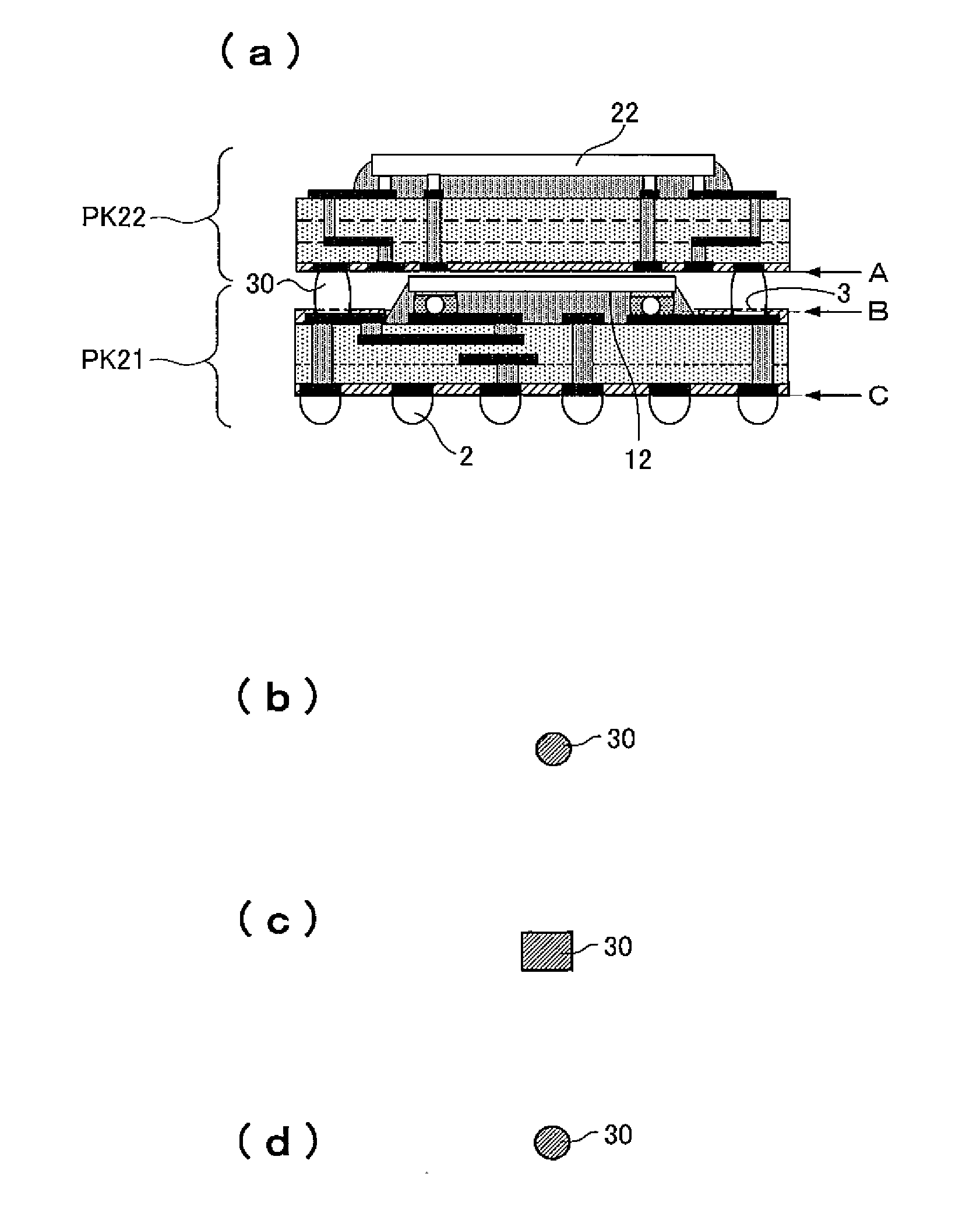
[0032]FIG. 1A shows a stacked semiconductor module according to the present invention. The numbers and shapes of terminals, electrodes, wires, and the like are omitted or are set such that they are easily shown in the drawings. Similar omissions and the like are made in all of the diagrams described below.

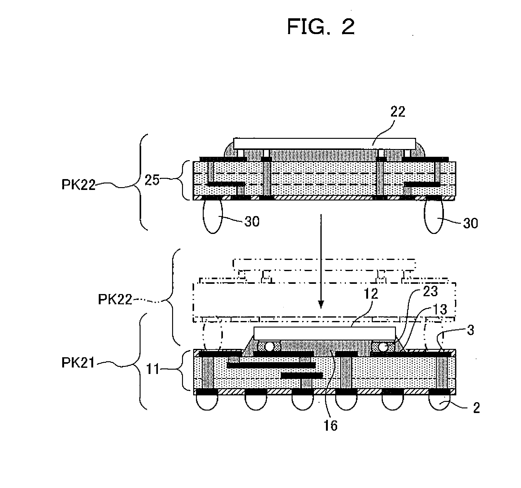
[0033]A second package PK22 is stacked and mounted on a first package PK21. A first semiconductor chip 12 is mounted on the upper surface of the first package PK21, and a second semiconductor chip 22 is mounted on the upper surface of a second substrate 25 of the second package PK22.

[0034]Specifically, the second package PK22 is a general-purpose memory device for stacking or the like, in which the second semiconductor chip 22 such as a memory is mounted on the substrate, electrodes are connected electrically by wire bonding or a flip-chip technique, and in some cases, the semiconduc...


PUM


Abstract

A pad (15) is provided on a surface connecting a first substrate (11) of a lower layer module with an upper layer module, the pad is partially covered by an insulating film (20) to form an opening section (3) exposing the pad (15), a first connection terminal (2) is formed on the lower surface of the first substrate (11) of the lower layer module, the planar shape of the opening section (3) is different from the planar shape of the first connection terminal (2), the outer shape of the opening section (3) is larger than the first connection terminal (2), and in a transmissive inspection from above, the shape of the lower end of a second connection terminal (30) spreading in the opening section (3) is not concealed by the other terminal. This configuration enables easy and reliable determination of whether bonding sections are satisfactory by a non-destructive inspection.

Description

BACKGROUND OF THE INVENTION[0001]1. Field of the Invention[0002]The present invention relates to a semiconductor module for stacking, which is disposed in a lowermost layer when a plurality of semiconductor devices are stacked together, and to a stacked semiconductor module using the same.[0003]2. Description of the Related Art[0004]With demands for miniaturization and improved functionality of electronic devices of various kinds, such as portable telephone devices or digital still cameras, stacked semiconductor modules (package on package) have been developed, in which electronic components, in particular, a plurality of semiconductor devices and chips are stacked together and united in a single body.[0005]In mounting of such a stacked semiconductor module, a connection yield between upper and lower packages due to ever higher density and ah improvement in inspection sensitivity in line with higher functionality have become an issue, and in response to this, an inspection yield has...

Claims


Application Information

Patent Timeline
Patent Type & Authority Applications(United States)
IPC IPC(8): H01L25/065H01L23/488H01L23/538
CPCH01L23/49811H01L23/49827H01L2225/1058H01L2225/1023H01L2224/32225H01L2924/15331H01L2924/15311H01L2924/15192H01L2924/01079H01L2924/01078H01L23/49838H01L25/105H01L2224/16225H01L2224/73204H01L2924/00H01L2224/16238H01L2224/05573H01L2224/05568H01L2224/05124H01L2224/05147H01L2224/05624H01L2224/05647H01L24/05H01L2924/00014
Inventor KAWABATA, TAKESHIYUI, TAKASHI
Owner PANASONIC CORP
Why Eureka
Try Eureka