Printing material profiles onto substrates

a technology of material profiles and substrates, applied in the field of printing, can solve the problems of increasing resistance in electrical conductors, introducing micro-cracks in wafers, shadow losses occurring in photovoltaic devices, etc., and achieve the effect of increasing the height of the material profil

Inactive Publication Date: 2010-12-02
MOSER BAER INDIA
View PDF3 Cites 2 Cited by
  • Summary
  • Abstract
  • Description
  • Claims
  • Application Information

AI Technical Summary

Benefits of technology

[0026]In addition, the printing apparatus does not require any contact with the substrate during printing, and therefore, does not exert pressure on the substrate.
[0027]Moreover, the printing apparatus does not require separate processes for printing a material profile of a desired width and increasing the height of the material profile. This makes the printing apparatus suitable for mass manufacturing.

Problems solved by technology

This is often referred to as shadow losses occurring in the photovoltaic device.
This may lead to increase in resistance in the electrical conductors.
Excessive pressure on a wafer may introduce micro-cracks in the wafer.
Moreover, the finger height may be inadequate, and has to be increased by another secondary process.
However, this technique also calls for inks of low viscosity.
The conventional techniques, therefore, suffer from one or more disadvantages.
This makes these techniques complex, tedious, and unsuitable for mass manufacturing.
In addition, fluids of different viscosity cannot be handled easily.

Method used


Image

  • Printing material profiles onto substrates
  • Printing material profiles onto substrates
  • Printing material profiles onto substrates

Examples


Embodiment Construction

[0040]As used in the specification and claims, the singular forms “a”, “an” and “the” include plural references unless the context clearly dictates otherwise. For example, the term “a syringe” may include a plurality of syringes unless the context clearly dictates otherwise. A term having “-containing” such as “metal-containing” contains a metal but is open to other substances, but need not contain any other substance other than a metal.

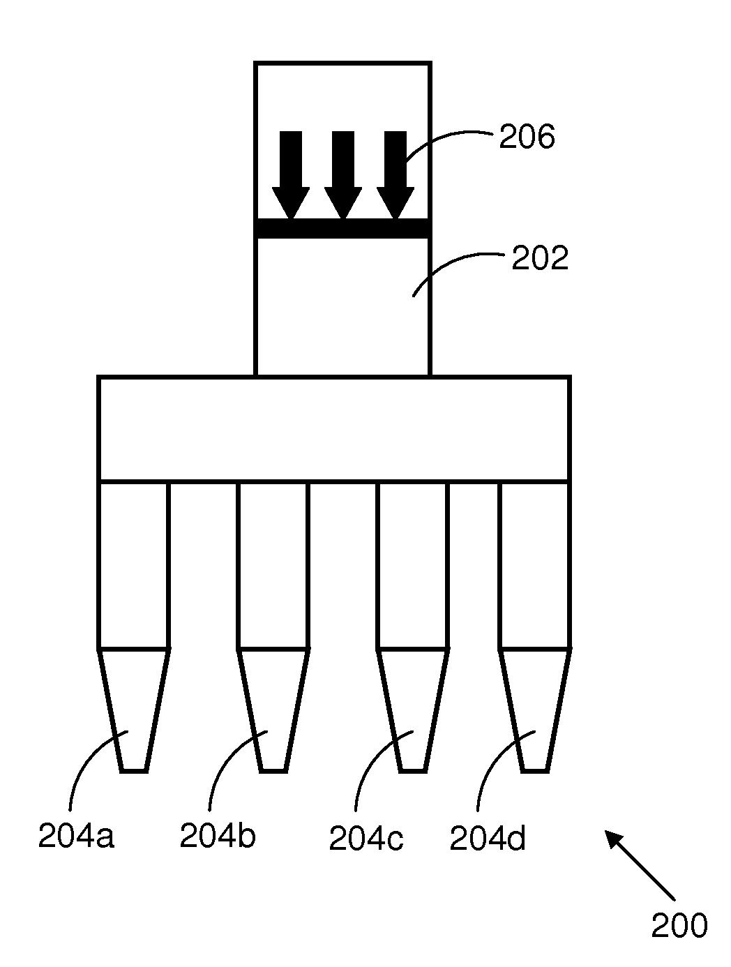
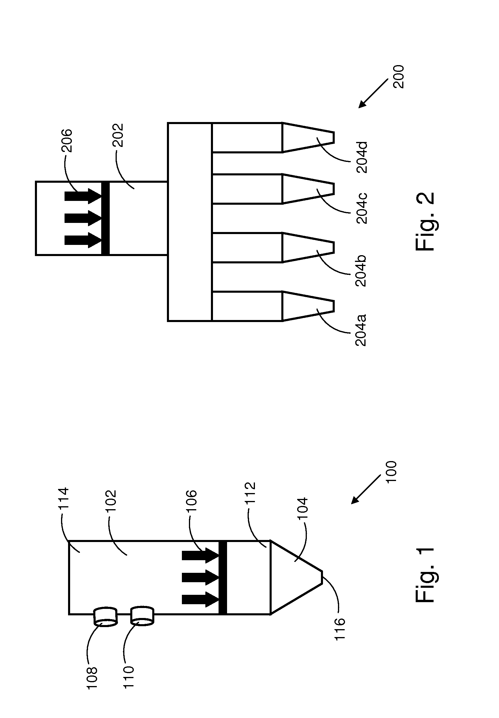
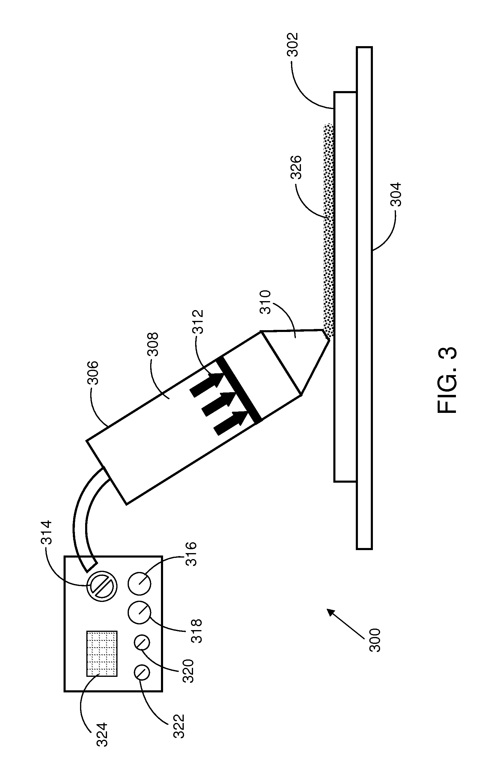
[0041]Embodiments herein provide a printing apparatus, method, system for printing a material profile onto a substrate. In the description herein for embodiments, numerous specific details are provided, such as examples of components and / or mechanisms, to provide a thorough understanding of embodiments. One skilled in the relevant art will recognize, however, that an embodiment can be practiced without one or more of the specific details, or with other apparatus, systems, assemblies, methods, components, materials, parts, and / or the like. In other in...


PUM


Abstract

A printing apparatus configured to print a material profile onto a substrate is provided. The printing apparatus includes a container, a nozzle, a positive displacement mechanism, and one or more regulators. The container is adapted to hold a precursor material. The container has a first end and a second end, with the nozzle connected to the first end of the container. The nozzle has an orifice configured to deposit the precursor material over the substrate. The positive displacement mechanism is configured to push the precursor material through the orifice of the nozzle over the substrate. The regulator is configured to deposit the precursor material in accordance with pre-determined parameters governing width and cross-sectional area of the precursor material deposited over the substrate, such that the precursor material deposited over the substrate has a pre-determined width and a pre-determined cross-sectional area.

Description

CROSS-REFERENCE TO RELATED APPLICATION[0001]This application claims the benefit of priority under 35 U.S.C 119 to co-pending Indian Patent Application No. 1263 / CHE / 2009 filed on Jun. 1, 2009. The entire disclosure of the prior applications is incorporated herein by reference.BACKGROUND OF THE INVENTION[0002]1. Field of the Invention[0003]The present invention relates, in general, to printing. More particularly, the present invention relates to a printing apparatus, method and system for printing a material profile onto a substrate of a photovoltaic device.[0004]2. Description of the Prior Art[0005]Photovoltaic devices convert solar energy into electrical energy by the photovoltaic effect. A typical photovoltaic device may be made by diffusing an n-type impurity in a p-type semiconductor wafer, or by diffusing a p-type impurity in an n-type semiconductor wafer. An anti-reflection coating may be applied on a front surface of the photovoltaic device to reduce reflection losses. The ant...

Claims


Application Information

Patent Timeline
Patent Type & Authority Applications(United States)
IPC IPC(8): B05C11/00
CPCB05B1/14B05C5/0216Y02E10/50H01L31/022425H01L21/6715
Inventor VERMA, AMITABH
Owner MOSER BAER INDIA
Why Eureka
Try Eureka