Touch Panel

a touch sensor and touch technology, applied in the field of touch panels, can solve the problems of difficult pressure application to the touch sensor, reduced visibility, and degraded image quality, and achieve the effect of improving durability and sensitivity of the touch sensor and reducing image quality

Inactive Publication Date: 2010-12-02
SEMICON ENERGY LAB CO LTD
View PDF46 Cites 106 Cited by
  • Summary
  • Abstract
  • Description
  • Claims
  • Application Information

AI Technical Summary

Benefits of technology

[0008]It is an object of one embodiment of the present invention to provide a touch sensor which can be formed over the same substrate as a display portion. Alternatively, it is an object of one embodiment of the present invention to provide a touch sensor which does not cause degradation in the quality of an image displayed on a display portion.
[0016]In one embodiment of the present invention, a touch sensor and a light-emitting element are disposed, so that it is possible to provide a thin touch panel with little degradation in image quality.
[0017]In one embodiment of the present invention, by using materials having different hardness for a filler layer, a partition wall, and a spacer, it is possible to provide a touch panel where data can be input efficiently and pressure is not applied to a light-emitting element easily. Further, by providing a spacer above a touch sensor, durability and sensitivity of the touch sensor can be improved.

Problems solved by technology

Thus, even if any high-definition display device is manufactured, visibility decreases and image quality degrades.
In contrast, in the case where a touch sensor is formed below an EL layer as in Reference 2, an image can be displayed at high definition; however, it is difficult to apply pressure to the touch sensor.
Thus, the touch sensor has a problem of the decrease in accuracy.

Method used


Image

  • Touch Panel
  • Touch Panel
  • Touch Panel

Examples


embodiment 1

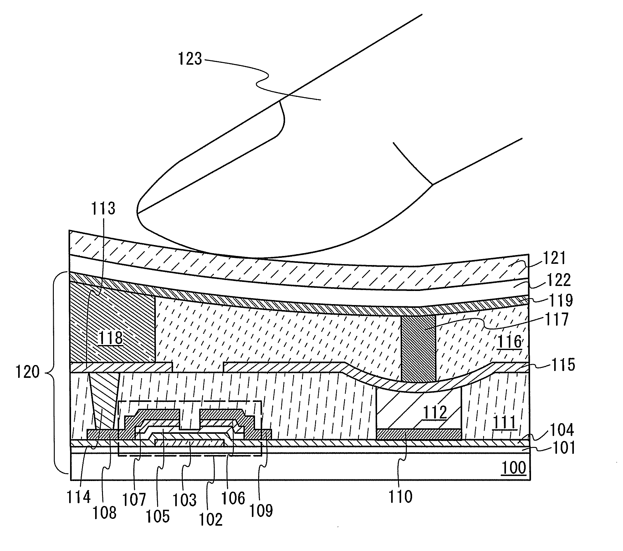
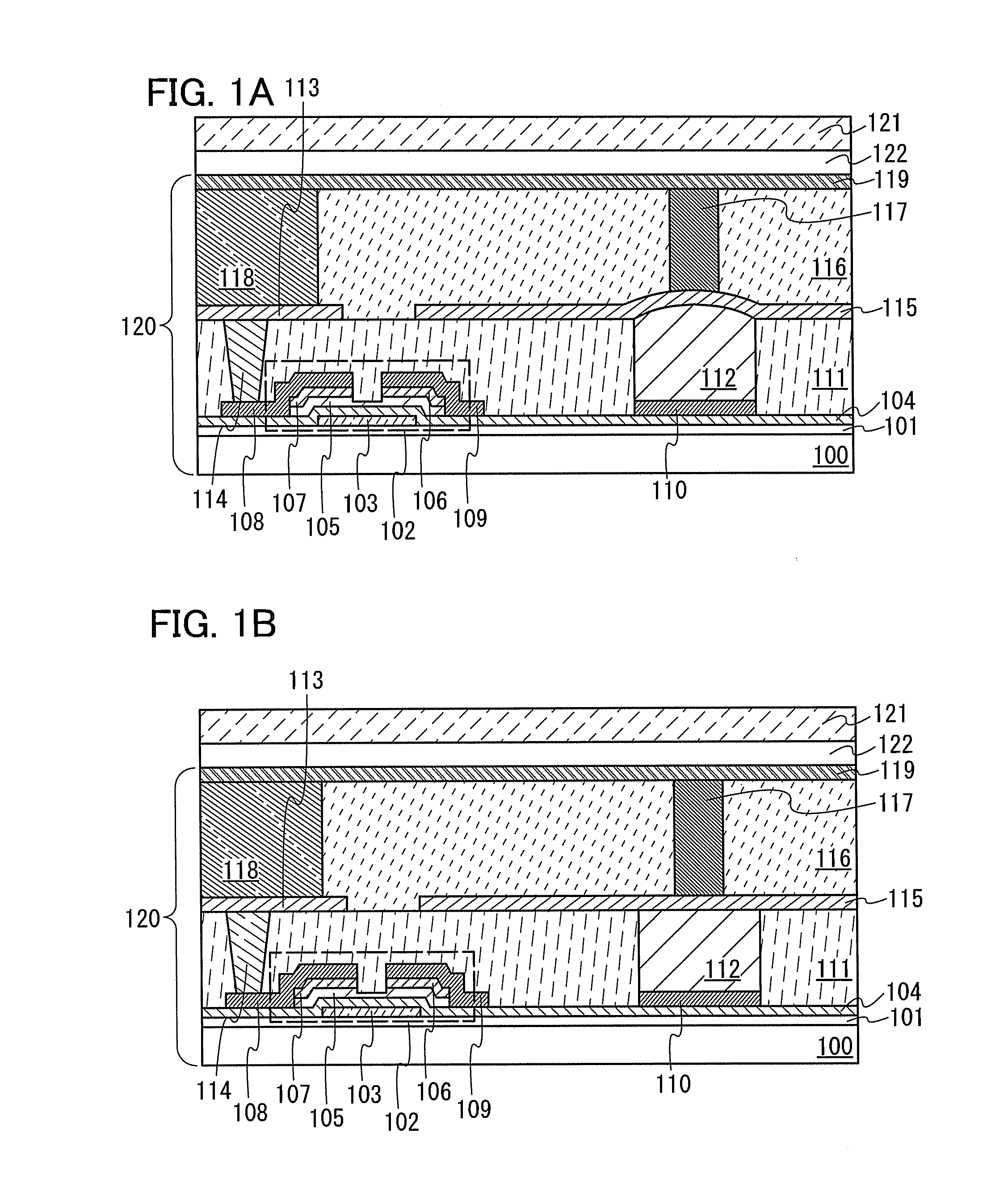
[0048]In this embodiment, structures of a touch panel of one embodiment of the present invention are described with reference to FIGS. 1A and 1B and FIG. 2.

[0049]A touch sensor is a device to which data is input when an upper electrode and a lower electrode are in contact with each other or the distance between the upper electrode and the lower electrode is changed, for example. In one embodiment of the present invention, a microelectromechanical system (MEMS) is used for the touch sensor.

[0050]MEMS is the abbreviation of a microelectromechanical system and is also simply called a micromachine. A micromachine generally refers to a micro device where “an electronic circuit having a semiconductor element” and “a movable microstructure having a three-dimensional structure” formed using a semiconductor microfabrication technology are integrated. Unlike the semiconductor element, the microstructure generally includes a movable portion.

[0051]The microstructure includes a structural layer ...

embodiment 2

[0067]In this embodiment, the operation of a capacitive type touch panel is described.

[0068]In a capacitive type touch sensor, data is input when the distance between an upper electrode and a lower electrode is changed. In one embodiment of the present invention, a microstructure (MEMS) is used for the touch sensor.

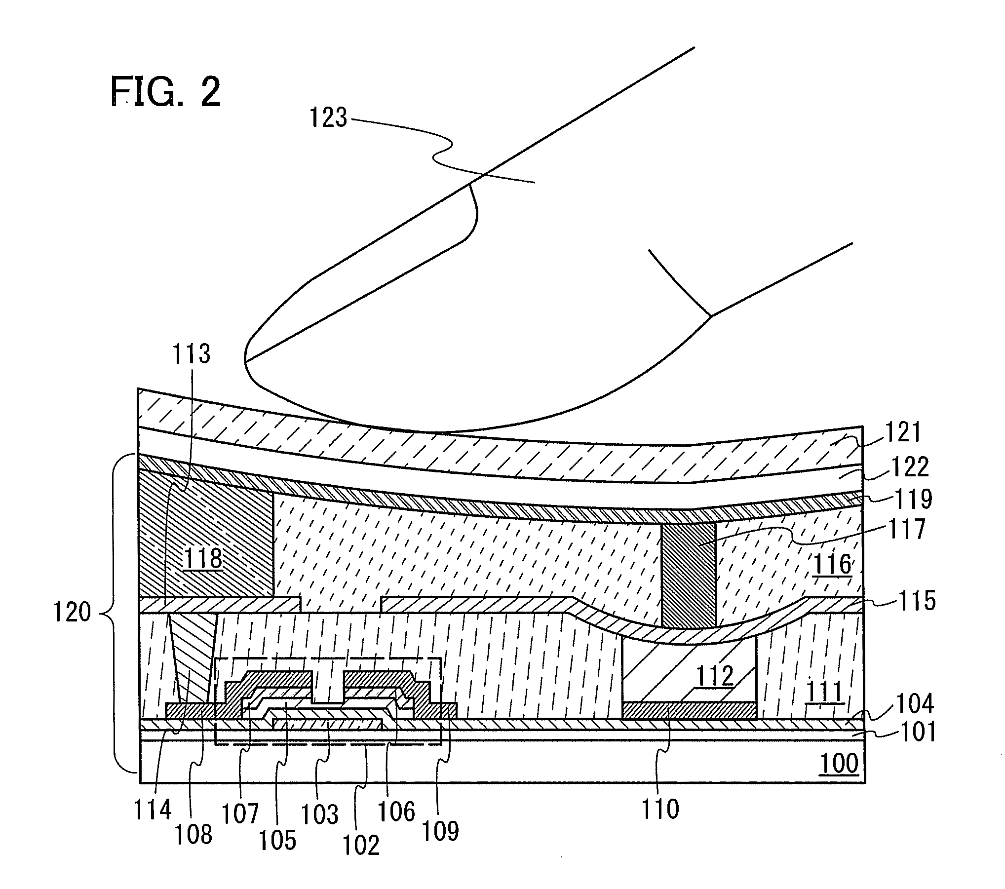
[0069]Since the structure of the touch sensor is as illustrated in FIGS. 1A and 1B and FIG. 2, description thereof is omitted here.

[0070]In the capacitive type touch panel, an insulating material which is a dielectric is provided between an upper electrode and a lower electrode. A deformable porous material or an elastic insulating material is used for the filler layer 112, which is the dielectric.

[0071]FIG. 3A illustrates one embodiment of one pixel included in the capacitive type touch panel. A top view of FIG. 3A is illustrated in FIG. 12 or FIG. 22, for example.

[0072]A gate of a switching transistor 200 is electrically connected to a gate line 201. One of a source and...

embodiment 3

[0078]In this embodiment, the operation of a capacitive type touch panel which is different from that in Embodiment 2 is described.

[0079]FIG. 3B illustrates one embodiment of one pixel included in the capacitive type touch panel. A top view of FIG. 3B is illustrated in FIG. 13 or FIG. 23, for example.

[0080]The switching transistor 200, the gate line 201, the source line 202, the first capacitor 203, the power supply line 204, the driving transistor 205, the light-emitting element 206, and the power supply line 207 are similar to those in FIG. 3A. A first terminal of a second capacitor 212 is electrically connected to the power supply line 204. A second terminal of the second capacitor 212 is electrically connected to a column line 213. The column line 213 is electrically connected to a row line 214.

[0081]Although two capacitors (touch sensors) whose capacitance values are changed are provided in FIG. 3A, one capacitor (touch sensor) whose capacitance value is changed is provided in ...


PUM


Abstract

A touch sensor (touch panel) which can be formed over the same substrate as a display portion is provided. Alternatively, a touch sensor (touch panel) which does not cause degradation in the quality of an image displayed on a display portion is provided. The touch panel includes a light-emitting element and a microstructure in which a pair of electrodes facing each other is isolated with an insulating material. As the insulating material, an elastic material or a material having a hole is used so that a filler layer formed using the insulating material can be deformed when a movable portion operates. It is preferable to use a material which is softened or hardened by certain treatment (e.g., heat treatment or chemical treatment) after formation.

Description

BACKGROUND OF THE INVENTION[0001]1. Field of the Invention[0002]The present invention relates to touch panels including touch sensors and display portions.[0003]2. Description of the Related Art[0004]In recent years, display devices including touch sensors have attracted attention. The display devices including touch sensors are referred to as touch panels, touch screens, or the like (hereinafter simply referred to as touch panels). Examples of the types of touch sensors include a resistive type, an acoustic pulse recognition type, a surface acoustic wave type, an infrared light-blocking type, a capacitive type, an electromagnetic induction type, an image recognition type, and the like. These types have different operating principles. In any type of touch sensor, data can be input when an object to be detected is in contact with a display device.[0005]A conventional touch sensor is formed over or below an EL layer including a light-emitting layer. In the case where a touch sensor is...

Claims


Application Information

Patent Timeline
Patent Type & Authority Applications(United States)
IPC IPC(8): H03K17/975H01L21/00G06F3/041
CPCG06F3/0412G06F3/0414H03K17/962H03K2217/9653H03K2217/96015H03K2217/96046H03K17/975G06F3/0446G06F3/0447
Inventor TAMURA, HIKARUKOZUMA, MUNEHIRO
Owner SEMICON ENERGY LAB CO LTD
Why Eureka
Try Eureka