Asterisk pad

Inactive Publication Date: 2010-12-02
TEXAS INSTR INC
View PDF4 Cites 26 Cited by
  • Summary
  • Abstract
  • Description
  • Claims
  • Application Information

AI Technical Summary

Benefits of technology

[0011]After realizing this possible source of epoxy voiding and device unreliability or failure, the inventor has developed a new semiconductor device design which, in one embodiment, comprises an etched leadframe chip pad. In an embodiment, one or more elongated features such as elongated grooves and/or dimples are etched into the chip pad which are oriented in a direction of the flow of epoxy across the chip pad as the chip is placed into the adhesive. The particular groove profile and orientation on the chip pad can reduce or eliminate air trapped within the dimple, and provide a more reliable device design.
[0012]In contrast with conventional hemispherical dimples, and without being limited by theory, it is believed tha

Problems solved by technology

The use of chip attach tape is a proven, but relatively expensive, die at

Method used


Image

  • Asterisk pad
  • Asterisk pad
  • Asterisk pad

Examples


Embodiment Construction

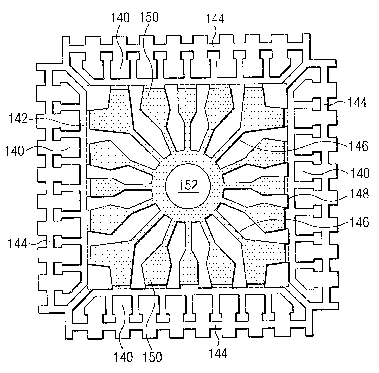
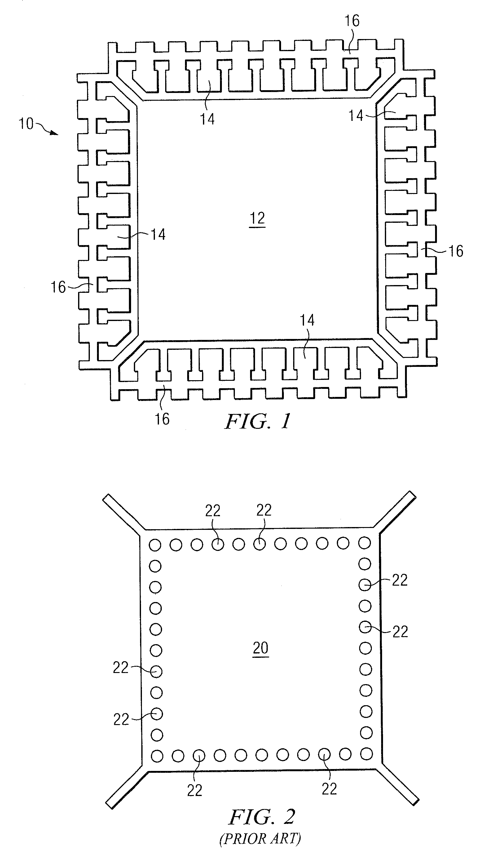
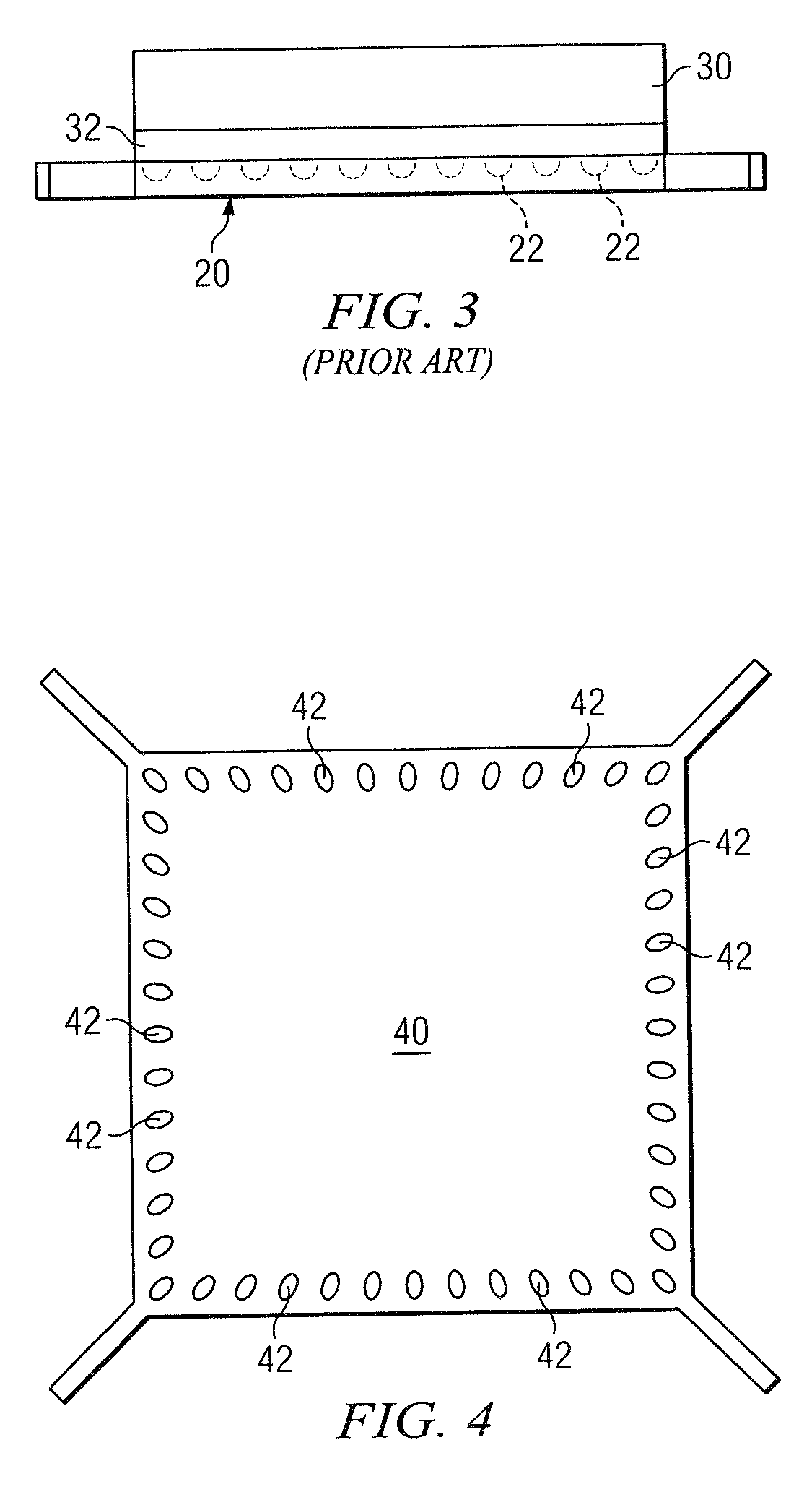
[0009]Attachment of a semiconductor chip to a chip pad using epoxy can have advantages over using chip attach tape. For example, in some semiconductor manufacturing processes, attachment of a chip to a chip pad with epoxy can be a simpler process requiring less expensive materials over a process which uses chip attach tape.

[0010]In contemplating the assembly of semiconductor devices, particularly the attachment of a chip to a chip pad, the inventor has realized that even though a chip pad having dimples can have advantages, epoxy voiding can result from the use of a such a chip pad. As previously discussed, dimples can be formed in an attempt to stabilize the position of the chip relative to the chip pad. During assembly, an amount of epoxy is dispensed onto the chip pad and the chip is placed into the epoxy with a controlled force. After examining a cross sectioned device having a hemispherical dimple, the inventor observed voids in the epoxy. It was determined that as the epoxy fl...


PUM


Abstract

A method and structure for a semiconductor device can include a chip support having a one or more elongated structures formed in the chip support The elongated structures, which have a width and a length greater than the width, receive chip attach material such as epoxy during a chip attach process. Because each elongated feature is oriented such that an axis through a center of the length of each elongated feature points to a center of the chip support, the chip attach adhesive flows into the feature with minimal trapping of air. Trapped air can cause delamination of the chip from the chip support, or cracking of the chip and device failure.

Description

FIELD OF THE INVENTION [0001]This invention pertains to the field of semiconductor devices, and more particularly to a method and structure for attachment of a semiconductor chip to a leadframe.BACKGROUND OF THE INVENTION [0002]A semiconductor device such as memory device, logic device, microprocessor, etc. can be packaged with conductive external connections to facilitate electrical coupling with test equipment, and eventual connection with a substrate such as a printed circuit board (PCB). Through-hole packages having leads which project through a printed circuit board, such as single in-line packages (SIPs) and dual in-line packages (DIPs), progressed to surface mount leads such as “j” style leads, which in turn progressed to surface mount connections such as flip chip and ball grid array (BGA) devices.[0003]Semiconductor device package styles include various types of leadframes to which a semiconductor chip (die, wafer section, etc.) is attached. Leadframe designs can comprise a...

Claims


Application Information

Patent Timeline
IPC IPC(8): H01L23/495H01L21/60
CPCH01L23/49503H01L23/49513H01L2924/10253H01L2924/01033H01L2924/01082H01L24/32H01L2224/27013H01L2224/32057H01L2224/32245H01L2224/83051H01L2224/83385H01L2924/3512H01L2924/00
Inventor ARSHAD, MOHAMAD ASHRAF BIN MOHD
Owner TEXAS INSTR INC
Why Eureka
Try Eureka