Pressure sensor and manufacturing method thereof

Inactive Publication Date: 2010-12-16
YAMATAKE HONEYWELL CO LTD
View PDF15 Cites 6 Cited by
  • Summary
  • Abstract
  • Description
  • Claims
  • Application Information

AI Technical Summary

Benefits of technology

[0025]The present invention enables, through the above, the pressure sensitive region to be made larger, enabling an improvement in

Problems solved by technology

That is, with high pressures (for example, 3 MPa or more), stresses are concent

Method used


Image

  • Pressure sensor and manufacturing method thereof
  • Pressure sensor and manufacturing method thereof
  • Pressure sensor and manufacturing method thereof

Examples


Example

Example of Embodiment 2

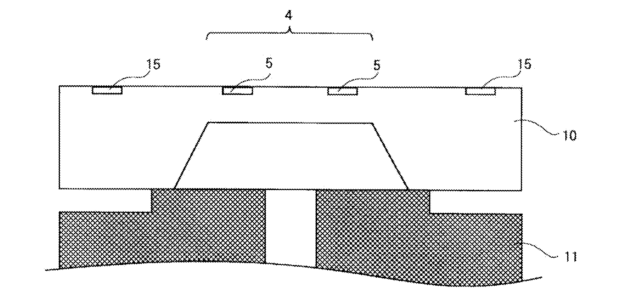
[0069]A specific form of embodiment to which the present invention is applied will be explained in detail, referencing the drawings. FIG. 4 is a side view cross-sectional diagram illustrating the structure of a pressure sensor as set forth in the present form of embodiment. FIG. 5 is a top view of the pressure sensor. FIG. 4 is a cross-sectional diagram along the section II-II in FIG. 5, where the pressure sensor as set forth in the present form of embodiment is a semiconductor pressure sensor that uses the semiconductor piezoresistance effect.

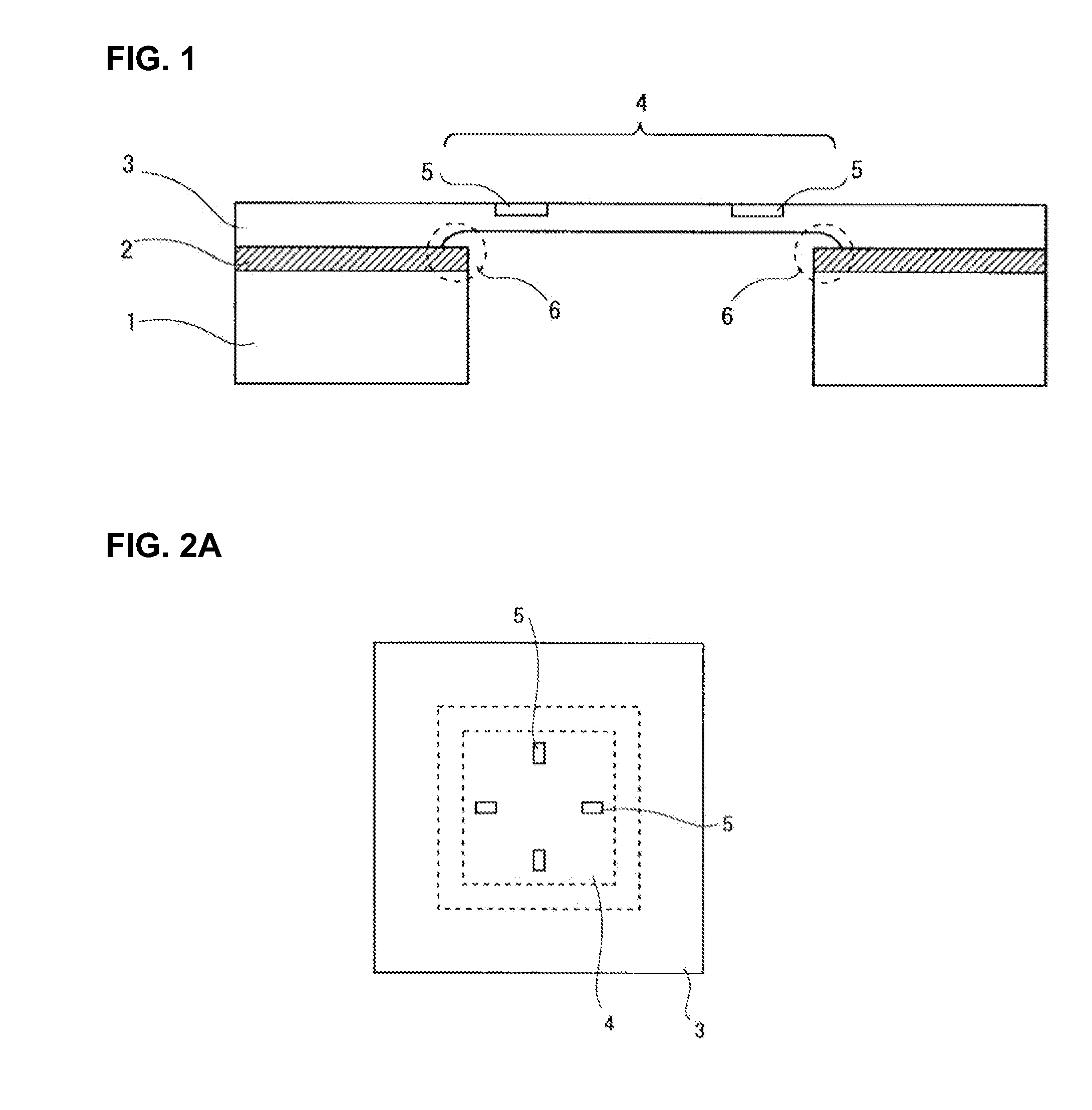
[0070]A pressure sensor 30 comprises a square sensor chip 10, made from an N-type single crystal silicon with the crystal plane orientation being the (100) plane, and a base11 to which the sensor chip 10 is bonded. The sensor chip 10 is provided with a first semiconductor layer 1 that serves as a substrate, an insulating layer 2, and a second semiconductor layer 3. That is, the sensor chip 10 has a three-layer structure ...


PUM


Abstract

A pressure sensor is provided with a sensor chip having a first semiconductor layer and a second semiconductor layer wherein a pressure-sensitive region is a diaphragm. In the pressure-sensitive region, an open section is formed on the first semiconductor layer, and a recessed section is formed on the second semiconductor layer in the pressure-sensitive region. The recessed section on the second semiconductor layer is larger than the opening section on the first semiconductor layer. An insulating layer may be arranged between the first semiconductor layer and the second semiconductor layer.

Description

CROSS REFERENCE TO PRIOR APPLICATIONS[0001]This application is a U.S. National Phase application under 35 U.S.C. §371 of International Application No. PCT / JP2008 / 069612, filed on Oct. 29, 2008 and claims benefit to Japanese Patent Application Nos. JP 2007-281988 and JP 2007-281989, filed on Oct. 30, 2007. The International Application was published in Japanese on May 7, 2009 as WO 2009 / 057620 under PCT Article 21(2). All these applications are herein incorporated by reference.FIELD OF THE INVENTION[0002]The present invention relates to a pressure sensor and to the method of manufacturing thereof, and, in particular, relates to a pressure sensor having a diaphragm, and to the method of manufacturing thereof.BACKGROUND OF THE INVENTION[0003]Pressure sensors that use the semiconductor piezoresistance effect are small, lightweight, and highly sensitive, and thus are used broadly in fields such as industrial instrumentation, medical care, and the like. In such pressure sensors, strain ga...

Claims


Application Information

Patent Timeline
IPC IPC(8): H01L29/84H01L21/302H01L21/50
CPCG01L9/0042G01L9/0054
Inventor TOKUDA, TOMOHISATOJO, HIROFUMI
Owner YAMATAKE HONEYWELL CO LTD
Why Eureka
Try Eureka