Split Path Sensing Circuit

a sensing circuit and path technology, applied in the field of split path sensing circuits, can solve the problems of increasing noise and process variation sensitivity, affecting the operation reducing the user's experience, so as to improve the tolerance of resistance based memory, improve the sensing margin, and improve the effect of operation

Active Publication Date: 2010-12-23
QUALCOMM INC +1
View PDF6 Cites 31 Cited by
  • Summary
  • Abstract
  • Description
  • Claims
  • Application Information

AI Technical Summary

Benefits of technology

[0008]One particular advantage provided by at least one of the disclosed embodiments is that operation of a resistance based memory may be improved by increasing a sensing margin of the resistance based memory as compared to conventional sensing circuits. The increased sensing margin may improve a tolerance of the resistance based memory to noise or process variation during read operations. Improved sensing margin may also lead to improved memory device yield.

Problems solved by technology

However, power consumption of such portable computing devices can quickly deplete a battery and diminish a user's experience.
Reducing power consumption has led to smaller circuitry feature sizes and operating voltages within such portable devices.
Such increased sensitivity to noise and process variations may be difficult to overcome when designing memory devices that use sense amplifiers.

Method used


Image

  • Split Path Sensing Circuit
  • Split Path Sensing Circuit
  • Split Path Sensing Circuit

Examples


Embodiment Construction

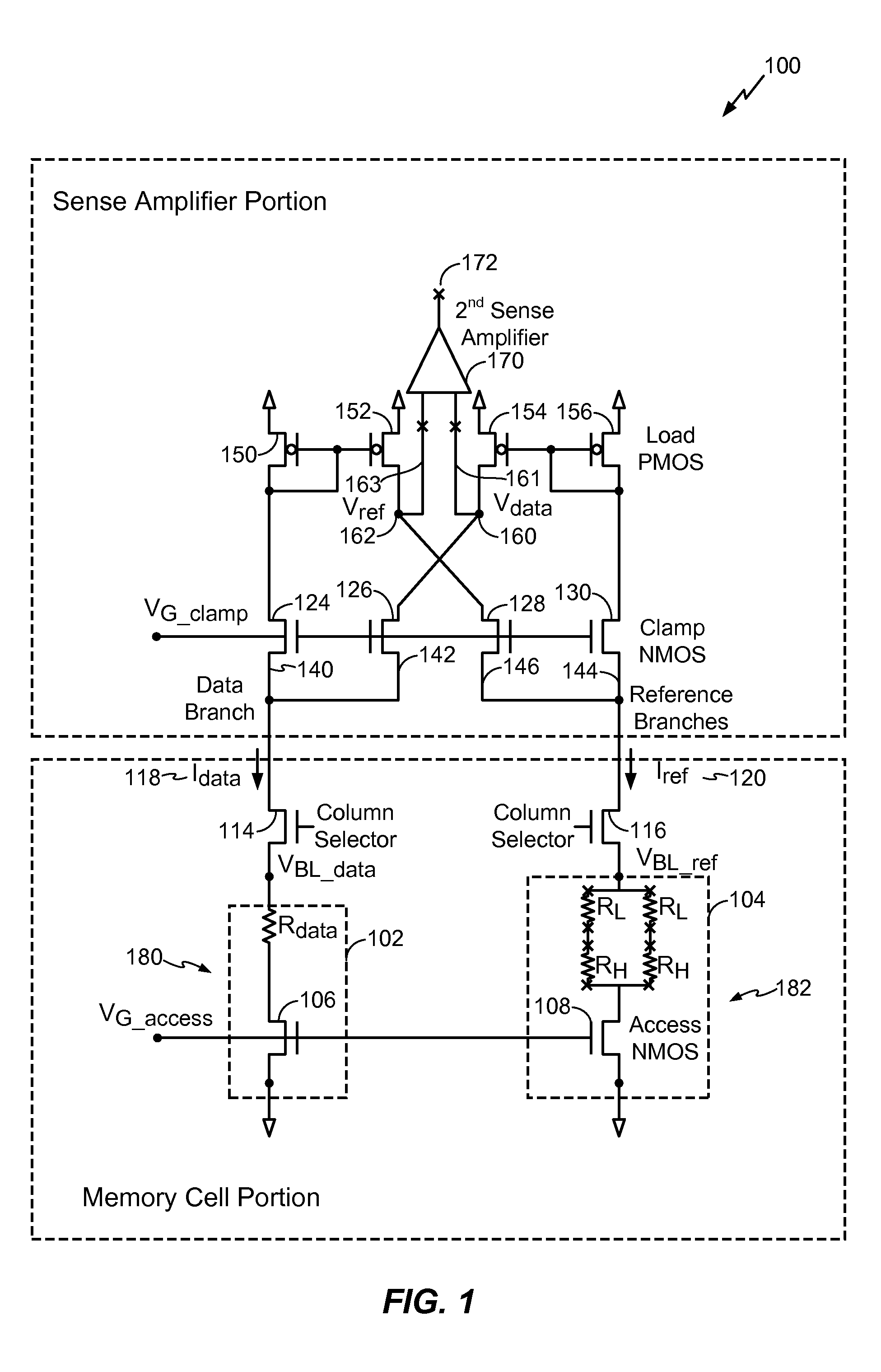
[0017]Referring to FIG. 1, a particular illustrative embodiment of a sensing circuit with a split path sense amplifier is depicted and generally designated 100. The sensing circuit 100 includes a first path 180 that includes a first resistive memory device 102 and a second path 182 that includes a second reference resistive memory device 104. In a particular embodiment, the first resistive memory device 102 is a magnetic tunnel junction (MTJ) device. Similarly, the reference resistive memory device 104 may be implemented, in a particular embodiment, as an MTJ device or a combination of MTJ devices storing predetermined values. In the particular embodiment shown in FIG. 1, the first path 180 includes a first column selector transistor 114 and a first access transistor 106. Similarly, the second path 182 includes a second column selector transistor 116 and a second access transistor 108. The first and second access transistors 106, 108 may be n-channel metal-oxide-semiconductor (NMOS)...


PUM


Abstract

A sensing circuit is disclosed. The sensing circuit includes a first path including a first resistive memory device and a second path including a reference resistive memory device. The first path is coupled to a first split path including a first load transistor and to a second split path including a second load transistor. The second path is coupled to a third split path including a third load transistor and to a fourth split path including a fourth load transistor.

Description

I. FIELD[0001]The present disclosure is generally related to a split path sensing circuit including a split path sense amplifier and a resistance based memory circuit.II. DESCRIPTION OF RELATED ART[0002]Advances in technology have resulted in smaller and more powerful personal computing devices. For example, there currently exist a variety of portable computing devices, including wireless computing devices, such as portable wireless telephones, personal digital assistants (PDAs), and paging devices that are small, lightweight, and easily carried by users. More specifically, portable wireless telephones, such as cellular telephones and Internet Protocol (IP) telephones, can communicate voice and data packets over wireless networks. Further, many such wireless telephones include other types of devices that are incorporated therein. For example, a wireless telephone can also include a digital still camera, a digital video camera, a digital recorder, and an audio file player. Also, such...

Claims


Application Information

Patent Timeline
Patent Type & Authority Applications(United States)
IPC IPC(8): G11C11/00G11C7/02
CPCG11C11/16G11C7/062G11C11/1673
Inventor JUNG, SEONG-OOKKIM, JISUKANG, SEUNG H.
Owner QUALCOMM INC
Why Eureka
Try Eureka