Compact millimeter wave packages with integrated antennas

a technology of integrated antennas and millimeter wave packages, which is applied in the direction of radiating element structural forms, resonant antennas, instruments, etc., can solve the problems of high cost, high cost, and high bulkiness of pointing antennas, and achieves the effects of low cost, high cost and high cos

Active Publication Date: 2010-12-30
GLOBALFOUNDRIES US INC +1
View PDF21 Cites 130 Cited by
  • Summary
  • Abstract
  • Description
  • Claims
  • Application Information

AI Technical Summary

Benefits of technology

[0003]Principles of the present invention provide techniques for compact millimeter wave packages with integrated antennas.

Problems solved by technology

These systems are often assembled using expensive and bulky waveguides and package-level or board-level microstrip structures to interconnect semiconductors and their required transmitter- or receiver-antennas.
However, high gain antennas for wireless video applications have very narrow beam widths, so pointing the antenna is very difficult for consumers.
However, packaging RF chips with integrated antennas or phased arrays is extremely difficult and very expensive due to the expensive components and extensive labor involved.

Method used


Image

  • Compact millimeter wave packages with integrated antennas
  • Compact millimeter wave packages with integrated antennas
  • Compact millimeter wave packages with integrated antennas

Examples


Embodiment Construction

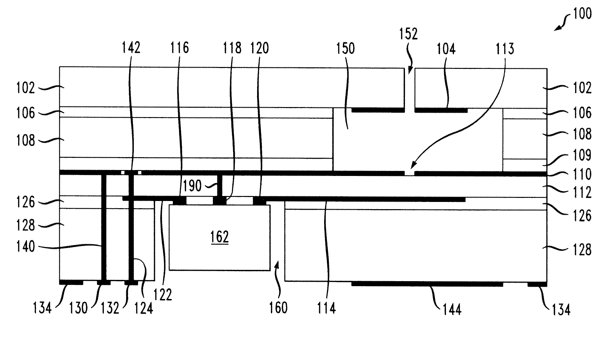
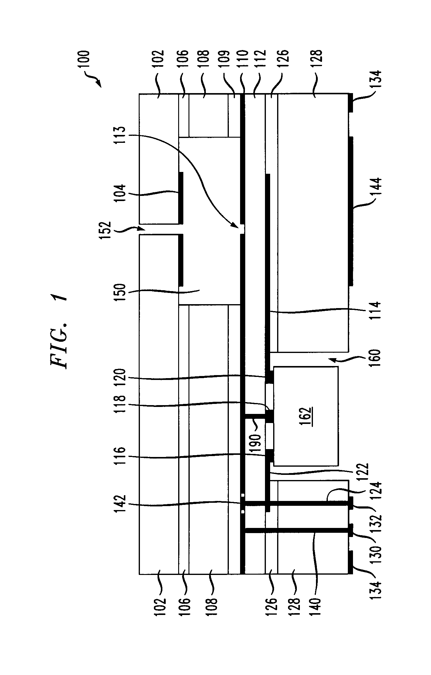
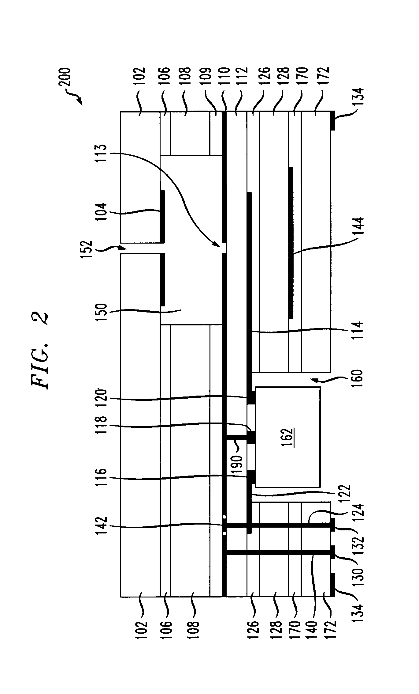
[0068]One or more embodiments of the invention provide an apparatus and method for low cost packages with integrated antennas and phased arrays operating in the millimeter wave (mmWave) range. An exemplary inventive package with integrated antennas is based on a multilayer printed circuit board (PCB). The package contains, for example, a rectangular or ring cavity for implementing high performance antenna(s) or antenna arrays and another cavity housing mmWave radio frequency (RF) integrated circuit chips. One or more embodiments of the invention also provide techniques to overcome the difficulties in making internal cavities and to avoid the need to employ wire bond technology at mmWave frequencies. Embodiments of the inventive packaging technology are consistent with the PCB manufacturing process and can be used for packages with an integrated antenna or antenna array.

[0069]Instances of the invention thus provide low cost packaging with integrated antennas or planar phased arrays; ...


PUM


Abstract

A radio-frequency integrated circuit chip package has at least one integrated antenna. The package includes at least one generally planar ground plane formed with at least one slot therein. A first substrate structure has an outer surface and an inner surface. The at least one generally planar ground plane is formed on the outer surface of the first substrate structure. At least one feed line is spaced inwardly from the ground plane and parallel thereto. The at least one feed line has an inner surface and an outer surface and is a transmission line formed on the inner surface of the first substrate structure with the outer surface of the at least one feed line adjacent the inner surface of the first substrate structure. At least one radio frequency chip is coupled to the feed line and the ground plane. A second substrate structure, spaced inwardly from the feed line, defines a chip-receiving cavity. The chip is located in the chip-receiving cavity. The inner surface of the at least one feed line borders the chip-receiving cavity. An antenna patch may be provided. Planar phased array embodiments, assemblies with motherboards and heat sinks, and fabrication techniques are also disclosed.

Description

FIELD OF THE INVENTION[0001]The present invention generally relates to communications circuitry, and, more particularly, to integrated circuit packages and antennas.BACKGROUND OF THE INVENTION[0002]In a wireless network, the connectivity and communication between devices is achieved through antennas attached to receivers or transmitters, in order to radiate the desired signals to or from other elements of the network. In radio communication systems, such as millimeter-wave radios, discrete components are usually assembled with low integration levels. These systems are often assembled using expensive and bulky waveguides and package-level or board-level microstrip structures to interconnect semiconductors and their required transmitter- or receiver-antennas. With recent progress in semiconductor technology and packaging engineering, the dimensions of these radio communication systems have become smaller. For applications such as wireless universal serial bus (USB), the operating dist...

Claims


Application Information

Patent Timeline
Patent Type & Authority Applications(United States)
IPC IPC(8): G06K19/06H01Q1/38H01L21/00
CPCG06K19/07749H01L23/66H01L2223/6627H01L2223/6677H01L2924/09701H01L2924/1903H01L2224/48227H01Q1/2283H01L2224/48091H01L2924/00014
Inventor CHEN, HO CHUNGFLOYD, BRIAN A.LIU, DUIXIAN
Owner GLOBALFOUNDRIES US INC
Why Eureka
Try Eureka