
Method of manufacturing liquid crystal display device

Active Publication Date: 2010-12-30
LG DISPLAY CO LTD
View PDF1 Cites 9 Cited by
  • Summary
  • Abstract
  • Description
  • Claims
  • Application Information

AI Technical Summary

Benefits of technology

[0022]An object of the present embodiment is to provide an LCD device manufacturing method that forms a common electrode and a contact hole exposing a drain electrode through one masking process so as to reduce the number of masks used in the formation of a thin film transistor.

Problems solved by technology

However, since the a-Si TFT has an electric mobility range of 1 Cm2 / Vsec, it is difficult to be used in peripheral circuits which operate by frequency signals of at least 1 MHz.
As such, a plurality of masking processes (i.e., photolithography processes) must be performed to manufacture the array substrate 10, thereby deteriorating the productivity of the LCD device.
Furthermore, the price of the mask used to form the desired pattern is very high.
As such, the manufacturing costs of the LCD device increase in proportion to the number of masks which are used in the manufacturing process.

Method used


Image

  • Method of manufacturing liquid crystal display device
  • Method of manufacturing liquid crystal display device
  • Method of manufacturing liquid crystal display device

Examples


Embodiment Construction

[0041]Reference will now be made in detail to the embodiments of the present disclosure, examples of which are illustrated in the accompanying drawings. These embodiments introduced hereinafter are provided as examples in order to convey their spirits to the ordinary skilled person in the art. Therefore, these embodiments might be embodied in a different shape, so are not limited to these embodiments described here. Also, the size and thickness of the device might be expressed to be exaggerated for the sake of convenience in the drawings. Wherever possible, the same reference numbers will be used throughout this disclosure including the drawings to refer to the same or like parts.

[0042]A method of manufacturing an LCD device according to an embodiment of the present disclosure will now be explained with reference to the attached drawings.

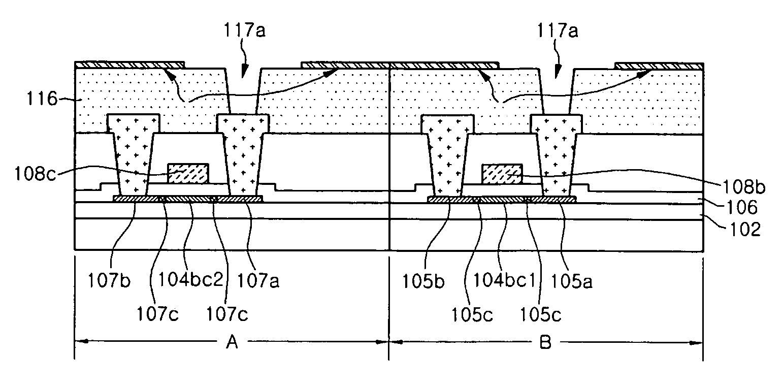
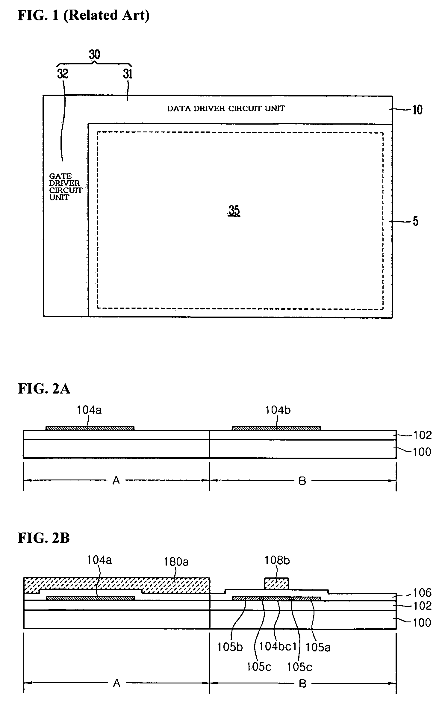
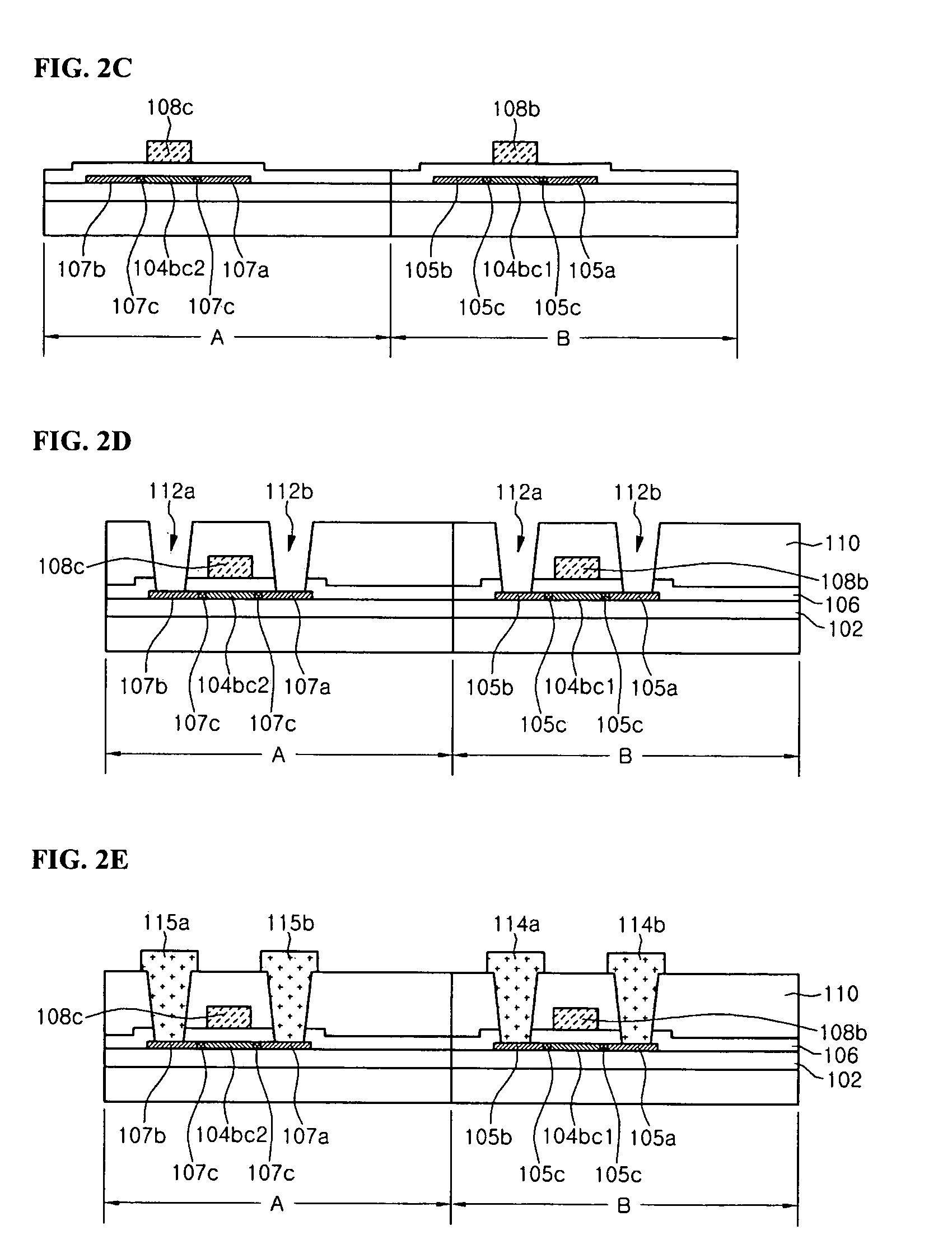
[0043]FIGS. 2A to 2H are cross-sectional views sequentially illustrating a method of manufacturing an LCD device according to an embodiment of the ...


PUM


Abstract

A method of manufacturing an LCD device is disclosed. The LCD device manufacturing method includes: forming first and second active patterns on P-channel and N-channel thin film transistor formation regions of a substrate using a first masking process, respectively; forming a first gate electrode on the P-channel thin film transistor formation region of the substrate using a second masking process; forming a second gate electrode on the N-channel thin film transistor formation region of the substrate using a third masking process; forming first contact holes partially exposing the respective N and P source regions and second contact holes partially exposing the respective N and P drain regions, using a fourth masking process; forming N and P source electrodes connected to the N and P source regions, and N and P drain electrodes connected to the N and P drain regions, using a fifth masking process; simultaneously forming third contact holes and a common electrode using a sixth masking process; forming fourth contact holes, which expose the respective N and P drain electrodes, using a seventh masking process; and forming a pixel electrode using a eighth masking process.

Description

CROSS-REFERENCE TO RELATED APPLICATION[0001]This application claims priority under 35 U.S.C. 119 to Korean Patent Application No. 10-2009-0058445, filed on Jun. 29, 2009, which is hereby incorporated by reference for all purposes as if fully set forth herein.BACKGROUND[0002]1. Field of the Disclosure[0003]This disclosure relates to a method of manufacturing a liquid crystal display device.[0004]2. Description of the Related Art[0005]Display devices have been largely highlighted in the recent information society as an important visual communication media. The display devices must meet the requirements of having low power consumption, slim size, light weight, high definition, and others, in order to highly occupy a market in future.[0006]Actually, liquid crystal display (LCD) devices corresponding to the main devices among current flat panel display (FPD) devices satisfy not only the requirements of the display device, but also have mass-productivity and improved performance. As such,...

Claims


Application Information

Patent Timeline
IPC IPC(8): H01L21/331
CPCG02F1/136227H01L27/1288H01L27/1214G02F2001/13625G02F1/13625H01L27/1274G02F1/136
Inventor LEE, SEOK WOOCHOI, SEUNG CHAN
Owner LG DISPLAY CO LTD
Features
  • Generate Ideas
  • Intellectual Property
  • Life Sciences
  • Materials
  • Tech Scout
  • Unparalleled Data Quality
  • Higher Quality Content
  • 60% Fewer Hallucinations
Learn More