Nozzle for high-speed jetting devices

Inactive Publication Date: 2010-12-30
KONINKLIJKE PHILIPS ELECTRONICS NV
View PDF7 Cites 18 Cited by
  • Summary
  • Abstract
  • Description
  • Claims
  • Application Information

AI Technical Summary

Benefits of technology

[0003]It is an object of the current invention to provide an imp

Problems solved by technology

The difficulty of this method is to provide good alignme

Method used


Image

  • Nozzle for high-speed jetting devices
  • Nozzle for high-speed jetting devices
  • Nozzle for high-speed jetting devices

Examples


Example

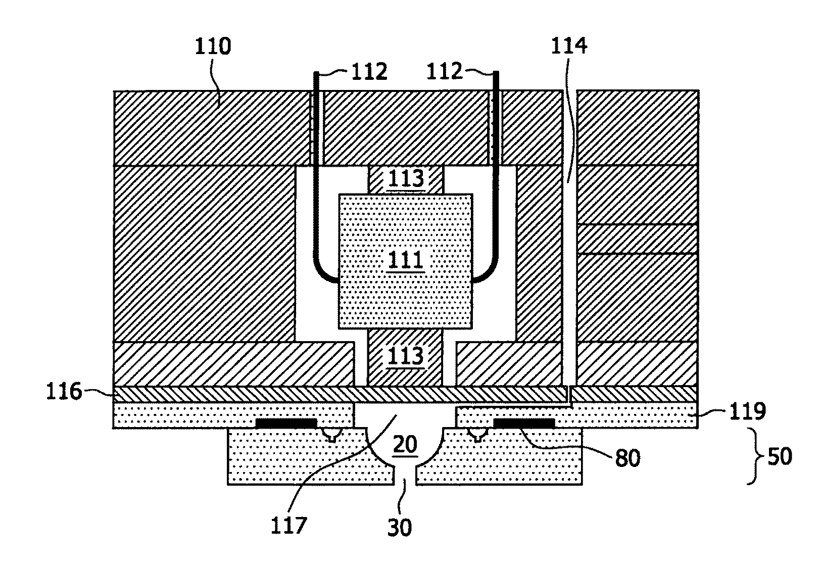
[0065]FIG. 18 shows a schematic drawing of a second embodiment of a nozzle 50 according the current invention, implemented in a high-speed ejection device. The high-speed ejection device comprises the nozzle 50, an actuation structure and a support structure. The nozzle 50 comprises a silicon substrate 1, an ejection chamber 20 and an ejection tube 30, both with a smoothened surface according to the description of FIG. 12. The actuation structure comprises a structured silicon base substrate 300, a first electrode layer 303 attached to the base substrate 300, a piezoelectric layer 302, such as e.g. Lead Zirconate Titanate (PZT), deposited on top of the first electrode layer 303 and a structured second electrode layer 301 deposited on top of the piezoelectric layer 302. The support structure comprises a silicon backing substrate 200 and several fixing structures 202, either deposited on the silicon backing substrate 200 or etched in the silicon backing substrate. The actuation struct...


PUM

PropertyMeasurementUnit
Angleaaaaaaaaaa
Pressureaaaaaaaaaa
Structureaaaaaaaaaa

Abstract

A nozzle for jetting devices is described comprising e.g. one patterned silicon substrate enabling semiconductor mass production. The method of manufacturing the nozzle is characterized by using one mask layer deposited on the silicon substrate. The etching of the silicon substrate is done by means of a first isotropic etching step and a second anisotropic etching step through the mask layer, resulting in a perfectly aligned nozzle.

Description

FIELD OF THE INVENTION[0001]The current invention is related to a method of manufacturing a nozzle for high-speed jetting devices for the ejection of a fluid, and to a nozzle for high-speed jetting devices.BACKGROUND OF THE INVENTION[0002]In U.S. Pat. No. 3,921,916, a method of manufacturing nozzles in monocrystalline silicon is disclosed. The method utilizes anisotropic etching through a silicon substrate to an integral etch-resistant barrier layer doped heavily with P-type impurities. The P-type layer is then etched through at the bottom of the previously etched structure to form a hole. The nozzle manufactured by this method comprises a nozzle body formed of a semiconductor material having a rectangular entrance aperture of a first cross-sectional area which tapers to a second cross-sectional area which is smaller than the cross-sectional area of said entrance aperture; and a membrane of said semiconductor material, formed within said second cross-sectional area and having an exi...

Claims


Application Information

Patent Timeline
IPC IPC(8): A61M3/02B23P17/00B05B1/00
CPCA61C17/02A61M5/30B41J2/1433Y10T29/494B41J2/162B41J2/1626B41J2002/14475B41J2/1606
Inventor NISATO, GIOVANNIROOZEBOOM, FREDDYRUBINGH, JAN-ERIC JACK MARTIJNDEKKERS, WOUTER
Owner KONINKLIJKE PHILIPS ELECTRONICS NV
Why Eureka
Try Eureka