Pixel circuit, driving circuit, light emitting apparatus, electronic apparatus and driving method of pixel circuit

a technology of electronic equipment and circuits, applied in the direction of instruments, computing, electric digital data processing, etc., can solve problems such as problems such as the error of electrical properties of driving transistors, the variation of elements, and the difference between target values, and achieve the effect of uniform properties of each transistor included in the pixel circui

Active Publication Date: 2011-01-06
ELEMENT CAPITAL COMMERCIAL CO PTE LTD
View PDF7 Cites 7 Cited by
  • Summary
  • Abstract
  • Description
  • Claims
  • Application Information

AI Technical Summary

Benefits of technology

[0008]An advantage of some aspects of the invention is to provide a pixel circuit, a driving circuit, a light emitti

Problems solved by technology

In a light emitting apparatus in which a driving transistor controls a driving current supplied to a light emitting element, an error (difference from a target value and variation between elements) of electrical properties of the driving transistor may be problem.
However, according to the technology disclosed in JP-A-2005-258407, since four or more TFTs are required per one pixel circuit and the large number of control signals and power sources is required, it is problematic in that a configuration for performing a compensation operation i

Method used


Image

  • Pixel circuit, driving circuit, light emitting apparatus, electronic apparatus and driving method of pixel circuit
  • Pixel circuit, driving circuit, light emitting apparatus, electronic apparatus and driving method of pixel circuit
  • Pixel circuit, driving circuit, light emitting apparatus, electronic apparatus and driving method of pixel circuit

Examples


first embodiment

A. First Embodiment

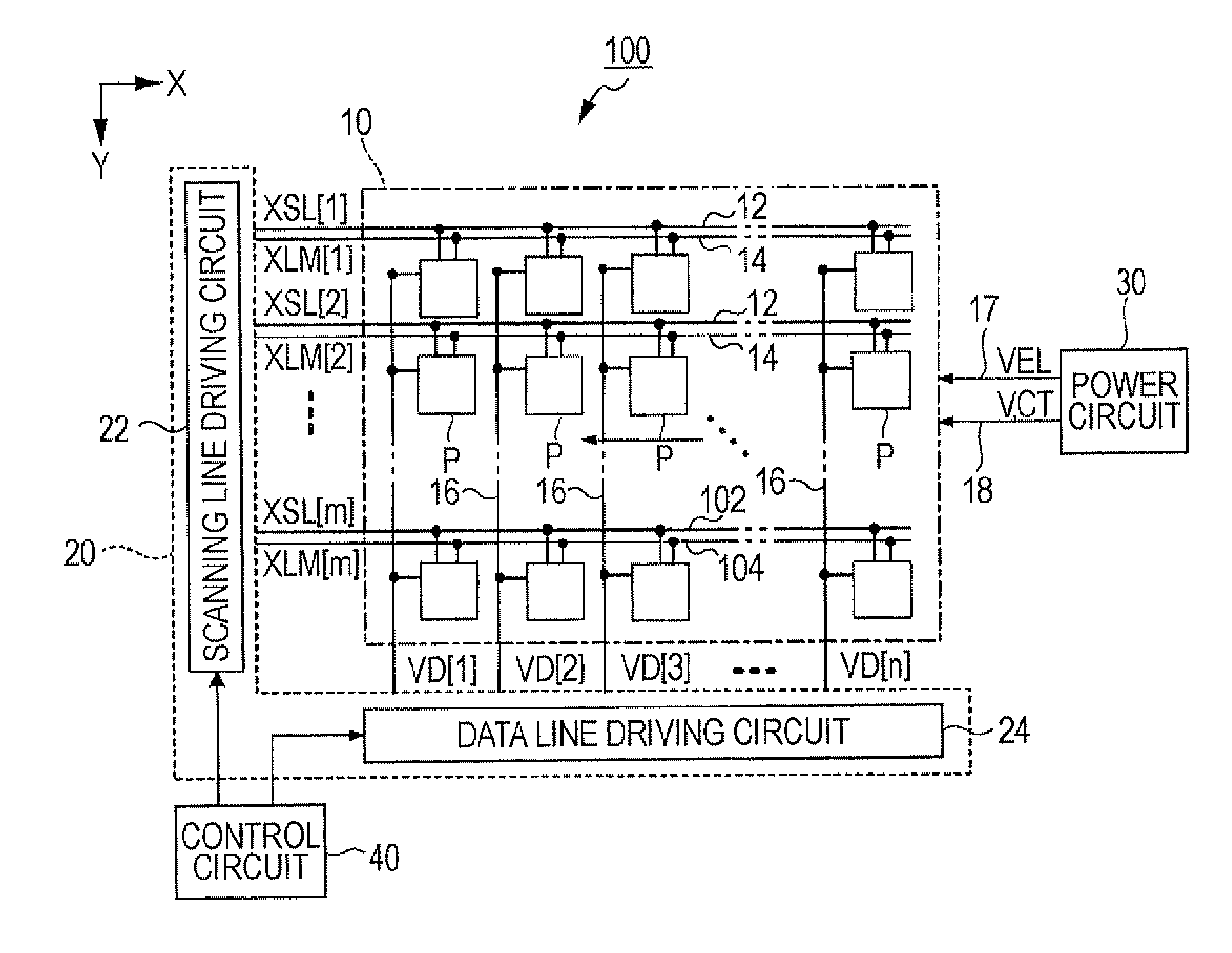
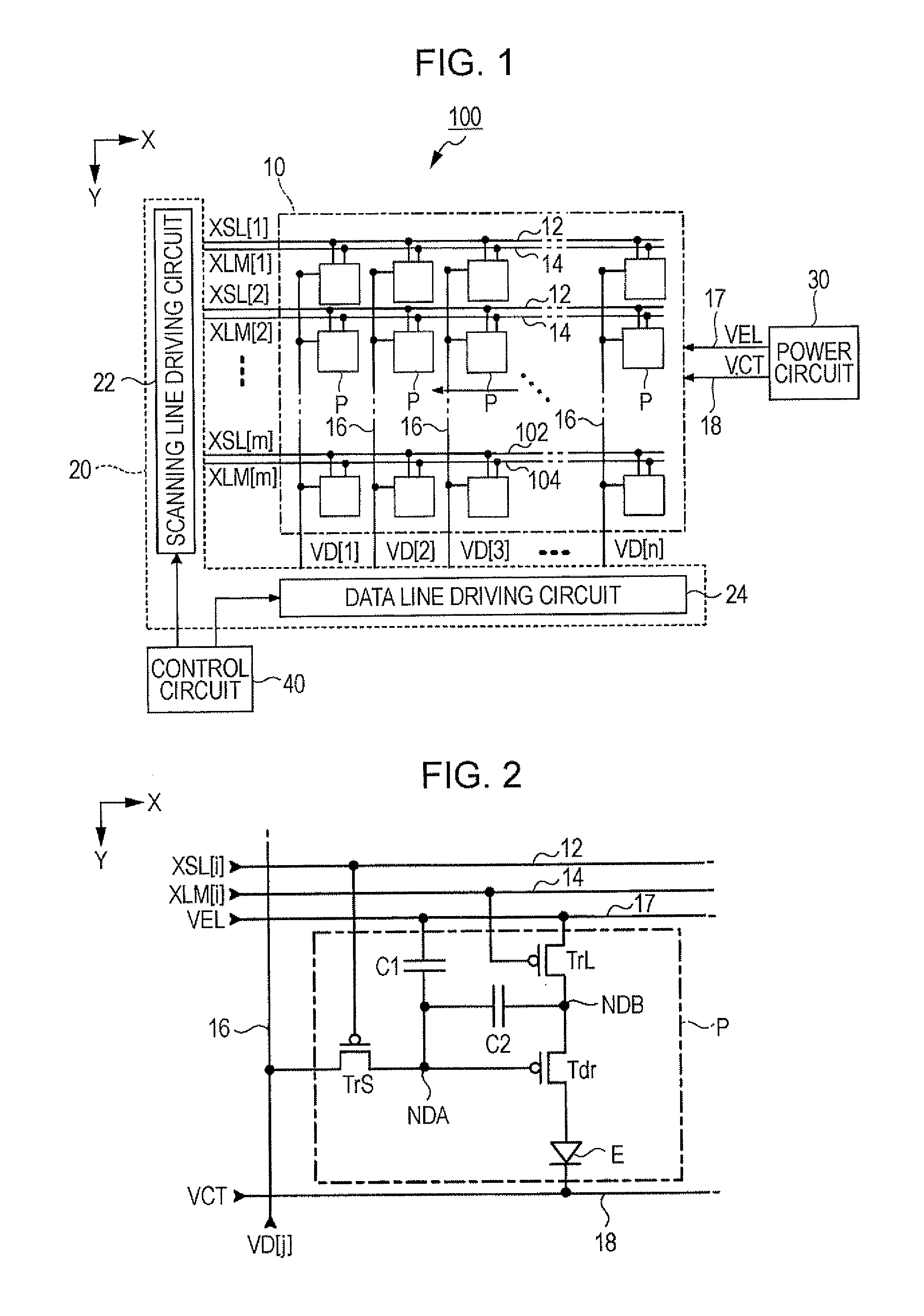
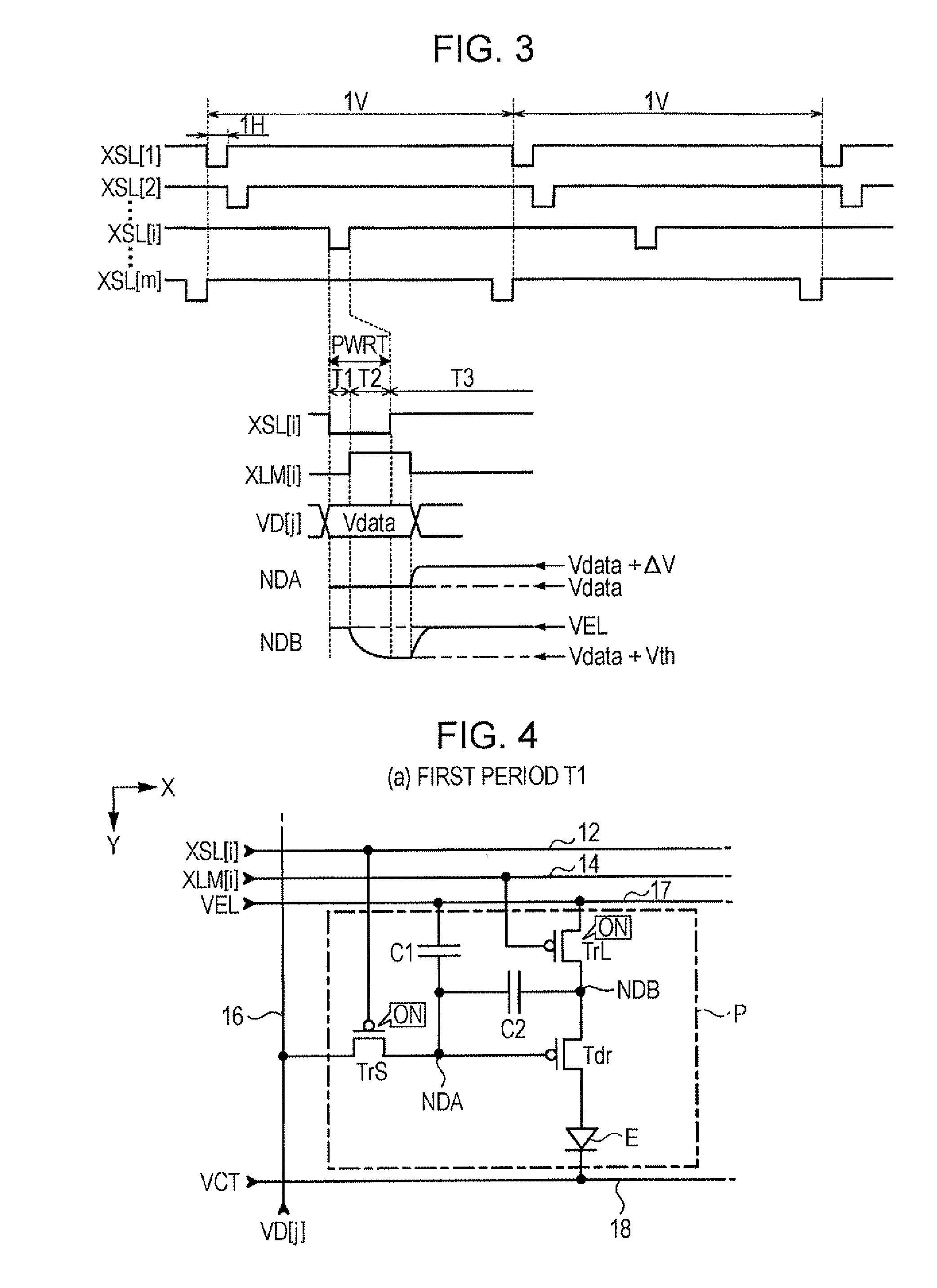
[0032]FIG. 1 is a block diagram illustrating a light emitting apparatus 100 according to the first embodiment of the invention. The light emitting apparatus 100 is mounted in an electronic apparatus as a display apparatus that displays an image. As shown in FIG. 1, the light emitting apparatus 100 includes a device unit 10 in which a plurality of pixel circuits P are arranged, a driving circuit 20 that drives each pixel circuit P, a power circuit 30 and a control circuit 40. In FIG. 1, the driving circuit 20, the power circuit 30 and the control circuit 40 are shown as separate circuits. However, it may be possible to employ a configuration in which a part or the whole of these circuits is designed as a single circuit.

[0033]The device unit 10 includes m scanning lines 12 extending in the X direction, m control lines 14 each extending in the X direction together with each scanning line 12 as a pair, and n data lines 16 extending in the Y direction perpendicular to ...

second embodiment

B. Second Embodiment

[0057]Since the second embodiment is substantially identical to the first embodiment, except that the control transistor TrL is set to an off state before the writing period PWRT starts and the power supplied to the node NDB is completely interrupted in the writing period PWRT, description about the same configuration will be omitted in order to avoid redundancy. FIG. 7 is a timing chart illustrating the operation of the light emitting apparatus 100 according to the second embodiment.

[0058]FIG. 7 will be described while focusing on an ith row. According to the embodiment, the period from the time point t prior to the start point is of the writing period PWRT by a predetermined time length to the end point to of the writing period PWRT is set as a second period T22. Further, the period before the second period T22 is set as a first period T11 and the period after the second period T22 is set as a third period T33.

[0059]In the first period T11, the control signal X...

modified example 1

1. Modified Example 1

[0066]According to the first embodiment as described above, all the transistors included in the pixel circuit P include a P channel type transistor. However, the invention is not limited thereto. For example, as shown in FIG. 10, all the transistors included in the pixel circuit P may include an N channel type transistor. FIG. 11 is a timing chart illustrating the operation of the light emitting apparatus 100 when all the transistors included in the pixel circuit P include the N channel type transistor. In the case of employing the N channel type transistor, a voltage relation (high and low) is reversed as compared with the case of employing the P channel type transistor. However, in such a case, since the essential operation is substantially identical to that of the previous embodiments, detailed description about the operation will be omitted. In addition, in FIGS. 10 and 11, similarly to the second embodiment, it is possible to set the control transistor TrL ...


PUM


Abstract

Disclosed is a pixel circuit including a light emitting element having one terminal and the other terminal, a driving transistor that supplies a driving current to the one terminal of the light emitting element, a first power line electrically connected to the other terminal of the light emitting element and receiving a first potential, a control transistor provided between a second power line, which receives a second potential, and a source of the driving transistor, and having a gate that receives a control signal through a control line, a first capacitor provided between the second power line and a gate of the driving transistor, a second capacitor provided between the gate and the source of the driving transistor, and a select transistor provided between a data line, which receives a data potential, and the gate of the driving transistor, and having a gate that receives a scanning signal through a scanning line.

Description

BACKGROUND[0001]1. Technical Field[0002]The present invention relates to a technology of driving a light emitting element such as an organic EL (Electroluminescence) element.[0003]2. Related Art[0004]In a light emitting apparatus in which a driving transistor controls a driving current supplied to a light emitting element, an error (difference from a target value and variation between elements) of electrical properties of the driving transistor may be problem. For example, JP-A-2005-258407 discloses a configuration of compensating for the difference of a threshold voltage of the driving transistor. FIG. 15 is a diagram illustrating the configuration of a pixel circuit disclosed in JP-A-2005-258407.[0005]However, according to the technology disclosed in JP-A-2005-258407, since four or more TFTs are required per one pixel circuit and the large number of control signals and power sources is required, it is problematic in that a configuration for performing a compensation operation is c...

Claims


Application Information

Patent Timeline
IPC IPC(8): G09G5/00
CPCG09G3/3233G09G2300/0819G09G2300/0861G09G2300/0852
Inventor JO, HIROAKI
Owner ELEMENT CAPITAL COMMERCIAL CO PTE LTD
Why Eureka
Try Eureka