Data writing method for flash memory and control circuit and storage system using the same

a data writing and control circuit technology, applied in the field of data writing methods, can solve the problems of inapplicability of flash memory storage devices, flash memory having a larger erasing unit, and unable to access the physical blocks in the system area or the replacement area, so as to avoid the problem of timeout and shorten the response time of writing data into the flash memory chip

Active Publication Date: 2011-01-06
PHISON ELECTRONICS
View PDF1 Cites 23 Cited by
  • Summary
  • Abstract
  • Description
  • Claims
  • Application Information

AI Technical Summary

Benefits of technology

[0009]Accordingly, the present invention is directed to a data writing method, wherein the response time of writing data into a flash memory chip is shortened so that the problem of timeout is avoided.

Problems solved by technology

Thus, a host system cannot access the physical blocks in the system area or the replacement area in general access states.
As a result, it takes a longer time to move the valid data in a physical block.
However, such a flash memory having a larger erasing unit may become inapplicable to a flash memory storage device (for example, a SD memory card) because the response time of a write command may exceed the specified response time of the flash memory storage device.

Method used


Image

  • Data writing method for flash memory and control circuit and storage system using the same
  • Data writing method for flash memory and control circuit and storage system using the same
  • Data writing method for flash memory and control circuit and storage system using the same

Examples


Embodiment Construction

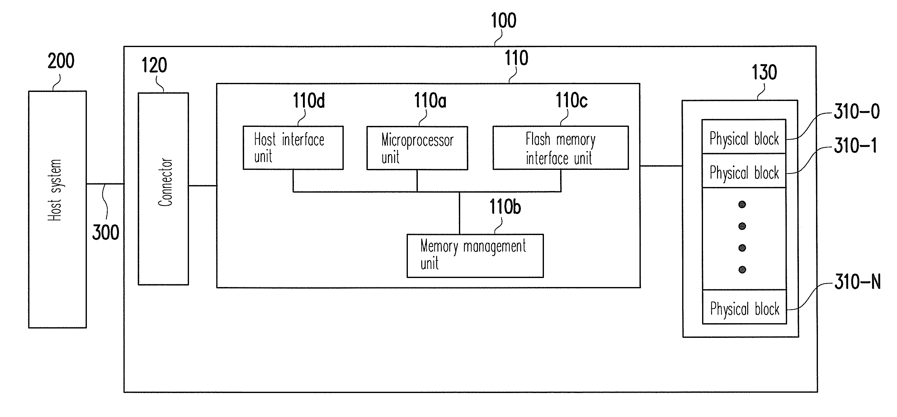
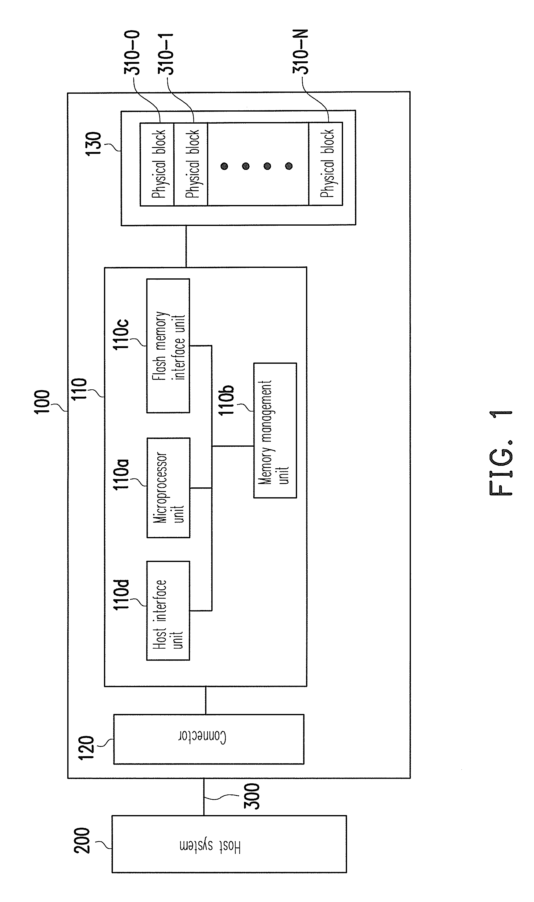
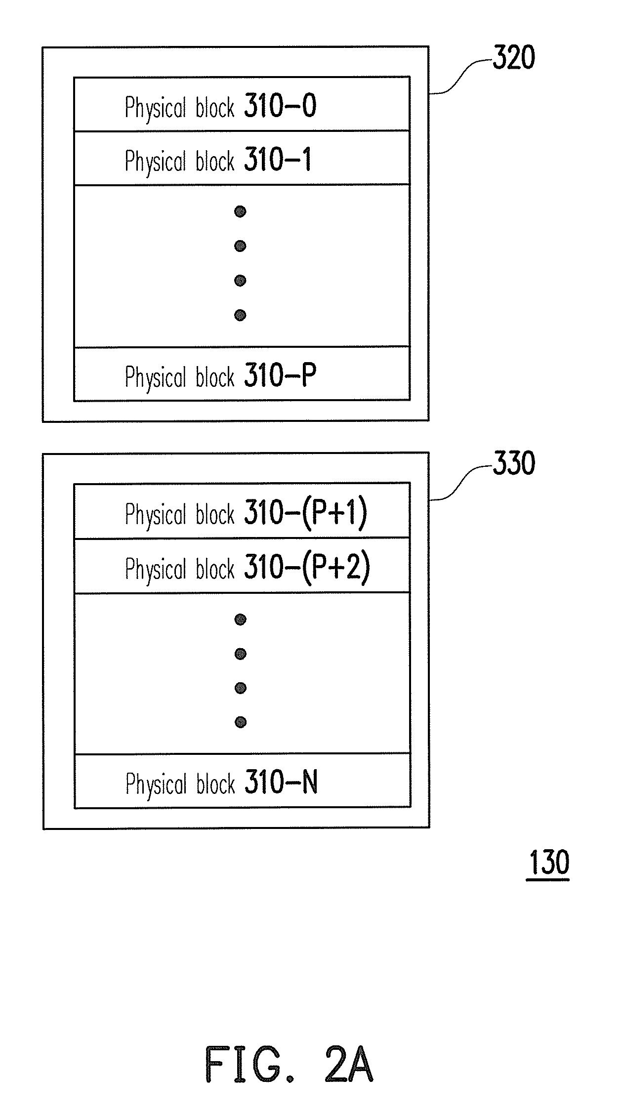
[0024]Reference will now be made in detail to the present preferred embodiments of the invention, examples of which are illustrated in the accompanying drawings. Wherever possible, the same reference numbers are used in the drawings and the description to refer to the same or like parts.

[0025]Embodiments of the present invention may comprise any one or more of the novel features described herein, including in the Detailed Description, and / or shown in the drawings. As used herein, “at least one”, “one or more”, and “and / or” are open-ended expressions that are both conjunctive and disjunctive in operation. For example, each of the expressions “at least on of A,B and C”, “at least one of A, B, or C”, “one or more of A, B, and C”, “one or more of A, B, or C” and “A, B, and / or C” means A alone, B alone, C alone, A and B together, A and C together, B and C together, or A, B and C together.

[0026]It is to be noted that the term “a” or “an” entity refers to one or more of that entity. As suc...


PUM


Abstract

A data writing method for a flash memory and a control circuit and a storage system using the same are provided. The data writing method includes determining whether the size of data to be stored by a host system is smaller than a predetermined value according to a write command received from the host system, when the size of the data is smaller than the predetermined value, the data is written into a corresponding buffer physical block or a corresponding spare buffer physical block. The data writing method further includes combining valid data belonging to the same logical block during the executions of several write commands. Accordingly, the response time during the execution of each write command is shortened, and the problem of timeout is avoided.

Description

CROSS-REFERENCE TO RELATED APPLICATION[0001]This application claims the priority benefit of Taiwan application serial no. 98122621, filed on Jul. 3, 2009. The entirety of the above-mentioned patent application is hereby incorporated by reference herein and made a part of specification.BACKGROUND[0002]1. Technology Field[0003]The present invention generally relates to a data writing method, and more particularly, to a data writing method which can shorten a response time, and a flash memory control circuit and a flash memory storage system using the same.[0004]2. Description of Related Art[0005]Along with the widespread of digital cameras, cell phones, and MP3 in recently years, the consumers' demand to storage media has increased drastically. Flash memory is one of the most adaptable memories for such battery-powered portable products due to its characteristics such as data non-volatility, low power consumption, small volume, and non-mechanical structure. A solid state drive (SSD) i...

Claims


Application Information

Patent Timeline
Patent Type & Authority Applications(United States)
IPC IPC(8): G06F12/02G06F12/00
CPCG06F2212/7203G06F12/0246
Inventor KHENG-CHONG, TAN
Owner PHISON ELECTRONICS
Why Eureka
Try Eureka