Field-effect transistor and method for fabricating field-effect transistor

Active Publication Date: 2011-01-13
RICOH KK
View PDF9 Cites 27 Cited by
  • Summary
  • Abstract
  • Description
  • Claims
  • Application Information

AI Technical Summary

Benefits of technology

[0014]Accordingly, embodiments of the invention attempt to provide a method for fabricating a field-effect transistor having an active layer mainly containing Mg and In capable of preventing damage to the active layer while patterning the active layer by etchin

Problems solved by technology

However, the TFTs having amorphous silicon or polysilicon as the active layer have their advantages and disadvantages, and hence it is difficult to simultaneously satisfy all the requirements.
In this case, however, since silicon needs to be treated at a relatively high temperature in a fabrication process, it is inappropriate to use silicon in the fabrication of TFTs in view of heat resistance of the substrate.
Accordingly, it is difficult to apply such a thin film to a large sized screen display.
However, evaluation of the field-effect transistor having the oxide semiconductor mainly composed of Mg and In as the active layer has shown that the active layer of the field-effect transistor is damaged while patterning the

Method used


Image

  • Field-effect transistor and method for fabricating field-effect transistor
  • Field-effect transistor and method for fabricating field-effect transistor
  • Field-effect transistor and method for fabricating field-effect transistor

Examples


Example

Example 1

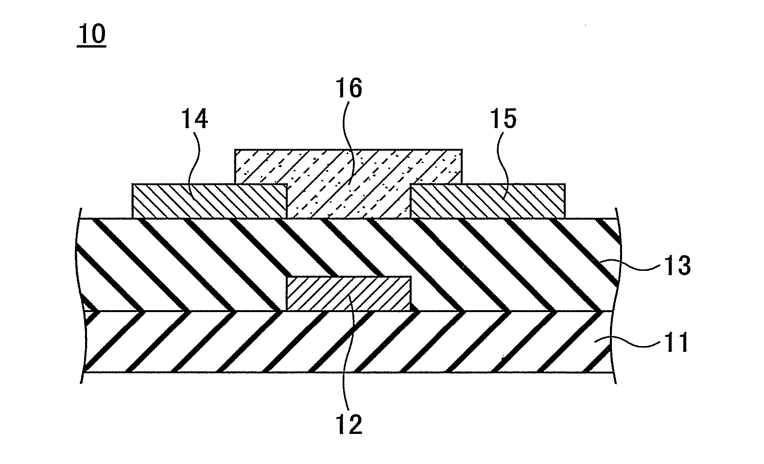
[0047]FIG. 4 is a flowchart illustrating a method for fabricating the field-effect transistor according to the embodiment in Example 1. In Example 1, the field-effect transistor 10 of FIG. 1 was fabricated by following steps S11 through S18, and characteristics of the field-effect transistor 10 were evaluated. Note that a field-effect transistor of Example 1 indicates the field-effect transistor 10 fabricated by following the steps S11 through S18 illustrated in FIG. 4.

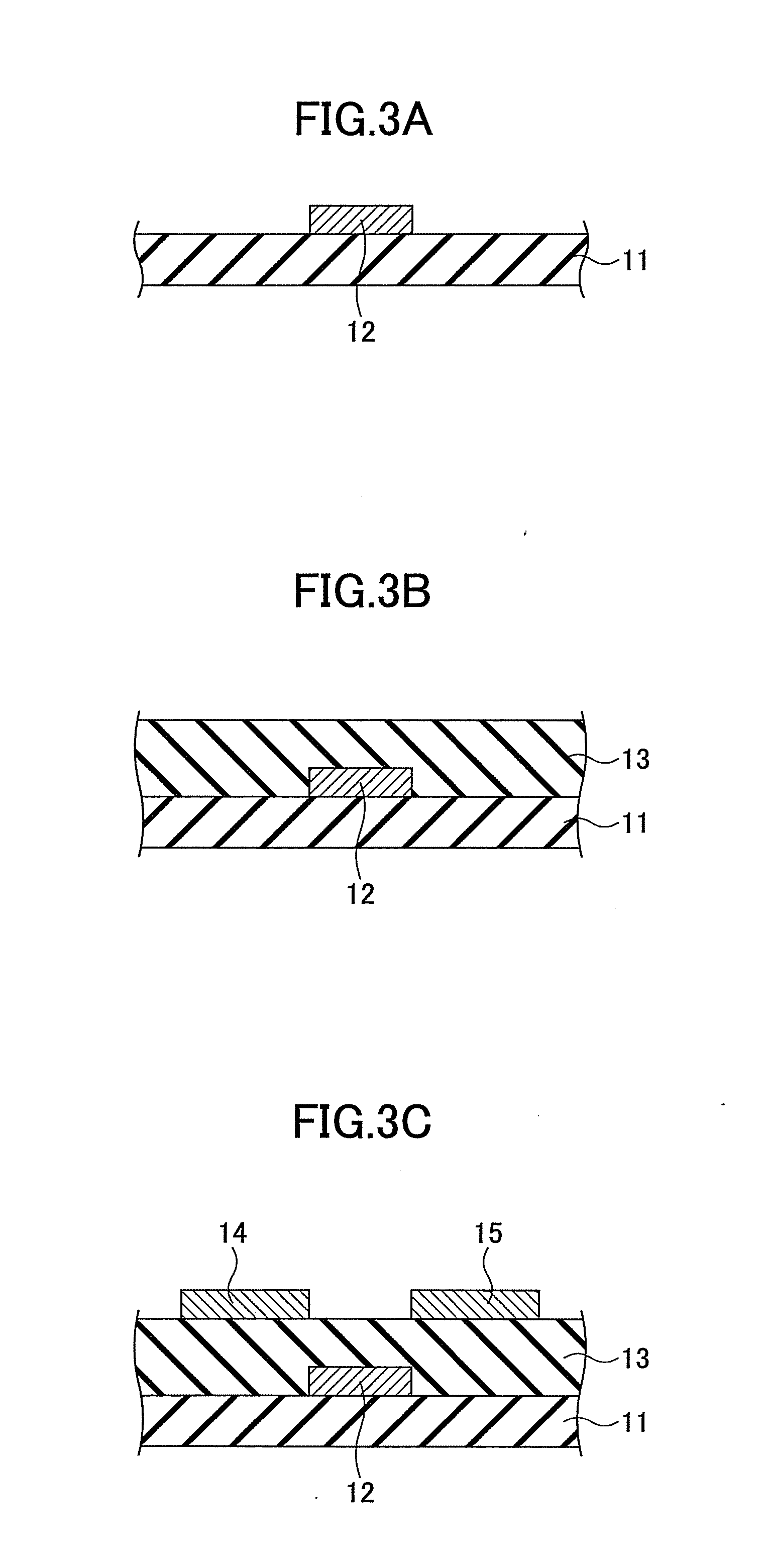
[0048]The method for fabricating the field-effect transistor of Example 1 is described below with reference to FIG. 4. In step S11, aluminum (Al) was deposited on the glass substrate 11 so as to have a deposited thickness of 100 nm. In step S12, the deposited aluminum (Al) was patterned in lines by etching and photolithography so as to form the gate electrode 12.

[0049]In step S13, SiO2 was deposited with a thickness of 200 nm by sputtering so as to form the gate insulating film 13 to cover the gate electrode ...

Example

Comparative Example 1

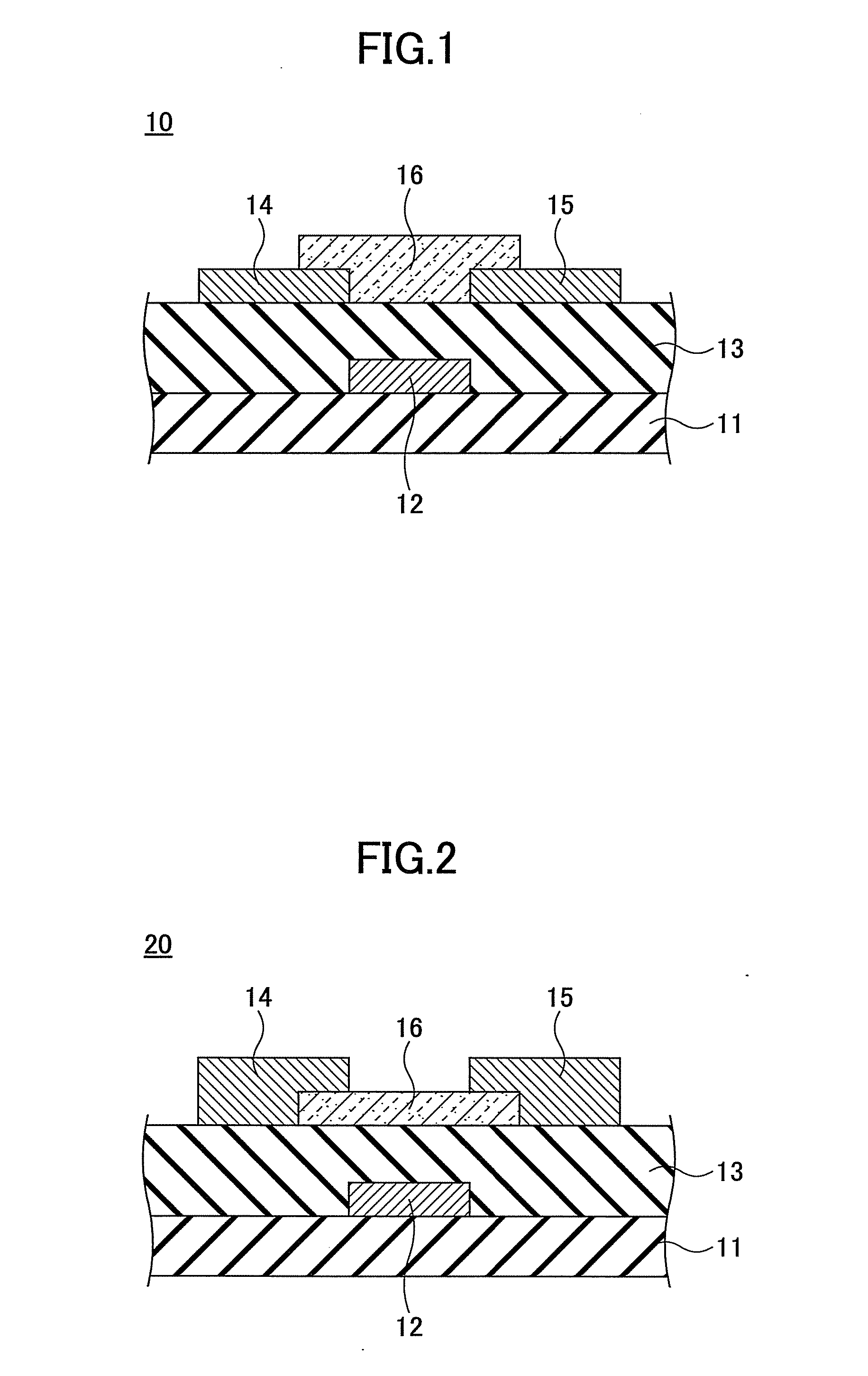
[0056]In Comparative Example 1, a field-effect transistor 10 of FIG. 1 was fabricated by following steps S11 through 17 illustrated in FIG. 4, and characteristics of the field-effect transistor 10 were evaluated. Note that the field-effect transistor of Comparative Example 1 indicates the field-effect transistor 10 fabricated by following the steps S11 through 17 illustrated in FIG. 4. The field-effect transistor of Comparative Example 1 differs from that of Example 1 in that the field-effect transistor of Comparative Example 1 was fabricated without carrying out the step S18 illustrated in FIG. 4.

[0057]FIG. 6 is a graph illustrating characteristics of the field-effect transistor of Comparative Example 1. FIG. 6 illustrates a relationship between a gate voltage V(G) and a source-drain current interval I(DS) in the field-effect transistor of Comparative Example 1 when a source-drain voltage V(DS) is set at 20 V. As illustrated in FIG. 6, the transistor did not sw...

Example

Comparative Example 2

[0059]FIG. 7 is a flowchart illustrating a method for fabricating the field-effect transistor of Comparative Example 2. In FIG. 7, the same reference numerals are assigned to steps identical to those of FIG. 4, and the descriptions thereof are omitted. Note that steps S27 and S28 in FIG. 7 are the same steps as steps S18 and S17 in FIG. 4, respectively. That is, FIG. 7 illustrates the flowchart in which step S17 and step S18 of the flowchart in FIG. 4 are conducted in a reverse order.

[0060]In Comparative Example 2, the field-effect transistor 10 of FIG. 1 was fabricated by following steps S11 through S16, S27 and S28 illustrated in FIG. 7, and characteristics of the field-effect transistor 10 were evaluated. Note that a field-effect transistor of Comparative Example 2 indicates the field-effect transistor 10 fabricated by following the steps S11 through S16, S27 and S28 illustrated in FIG. 7. The field-effect transistor of Comparative Example 2 differs from that...


PUM


Abstract

A method for fabricating a field-effect transistor having a gate electrode, a source electrode, a drain electrode, and an active layer forming a channel region, the active layer having an oxide semiconductor mainly containing magnesium and indium is disclosed. The method includes a deposition step of depositing an oxide film, a patterning step of patterning the oxide film by processes including etching to obtain the active layer, and a heat-treatment step of heat-treating the obtained active layer subsequent to the patterning step.

Description

BACKGROUND OF THE INVENTION[0001]1. Field of the Invention[0002]The invention generally relates to a field-effect transistor including an active layer having an oxide semiconductor, and a method for fabricating the field-effect transistor.[0003]2. Description of the Related Art[0004]The field-effect transistor (FET) is a transistor that controls current between a source electrode and a drain electrode based on the principle of applying a voltage to agate electrode to generate an electric field in a channel, whereby the gate is provided for the flows of electrons or holes. Based on the characteristics of FET, the FET is generally used as a switching device or amplifier device. The FET generally has a low gate current and a planar structure, which facilitate the fabrication or integration of the FET easier than a bipolar transistor. Accordingly, the FET is considered as one of the critical devices among the currently available integrated circuits in electronic devices. The FET may be ...

Claims


Application Information

Patent Timeline
IPC IPC(8): H01L29/786H01L21/36
CPCH01L21/02565H01L29/66969H01L29/7869H01L21/02631H01L21/324H01L29/66742
Inventor ABE, YUKIKOUEDA, NAOYUKINAKAMURA, YUKISONE, YUJI
Owner RICOH KK
Why Eureka
Try Eureka