Optical waveguide, opto-electronic circuit board, and method of fabricating opto-electronic circuit board
a technology optical waveguides, which is applied in the direction of instruments, cladded optical fibres, optical elements, etc., can solve the problems of difficult to sufficiently satisfy the demands, the fabrication process of opto-electronic circuit boards becomes complex, and the size of optical waveguides is reduced, so as to improve the performance and productivity of opto-electronic circuit boards. , the effect of reducing the size of the optical waveguid
- Summary
- Abstract
- Description
- Claims
- Application Information
AI Technical Summary
Benefits of technology
Problems solved by technology
Method used
Image

Examples
first embodiment
[0029]FIGS. 3A through 3C are cross sectional views illustrating examples of an optical waveguide in a first embodiment of the present invention and a modification of the first embodiment. An optical waveguide 20A of the first embodiment illustrated in FIGS. 3A and 3B and an optical waveguide 20B of the modification of the first embodiment illustrated in FIG. 3C both include a first optical waveguide part 23 in which first cores 22a are bonded to a first clad layer 21a, and a second optical waveguide part 24 in which second cores 22b are bonded to a second clad layer 21b. The first optical waveguide 23 and the second optical waveguide 24 are integrally formed via a common clad layer 25 that directly covers the first cores 22a of the first optical waveguide 22 and the second cores 22b of the second optical waveguide 24.
[0030]In some of the figures, the cores 22a and 22b are illustrated without hatchings for the sake of convenience, in order to more clearly illustrate the optical path...
second embodiment
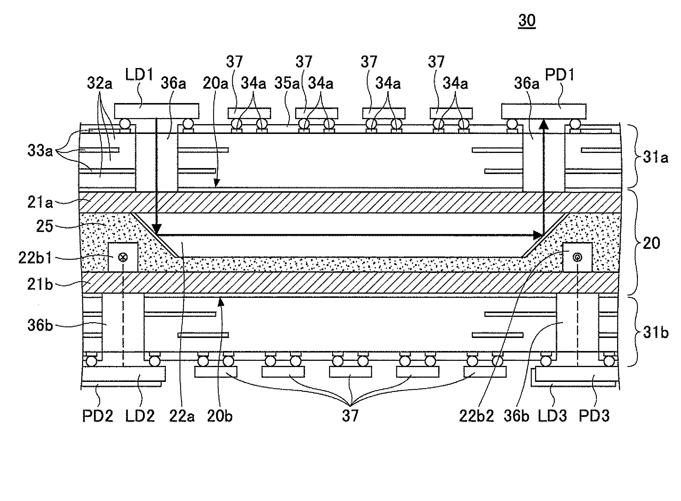
[0042]FIG. 4 is a cross sectional view illustrating an example of the opto-electronic circuit board in a second embodiment of the present invention. In FIG. 4, those parts that are the same as those corresponding parts in FIGS. 3A and 3B are either designated by the same reference numerals or the designation by the same reference numerals is omitted, and a description thereof will be omitted.
[0043]FIG. 4 illustrates an example in which an opto-electronic circuit board 30 has electrical circuit layers 31a and 31b that are respectively stacked on front and back (or upper and lower) surfaces of an optical waveguide 20. An optical signal emitted from a light emitting element LD1, such as a laser diode, provided on the electrical circuit layer 31a propagates in an optical path that passes through a core 22a and reaches a light receiving element PD1, such as a photodiode, provided on the electrical circuit layer 31a, as illustrated by arrows. In FIG. 4, the opto-electronic circuit board 3...
third embodiment
[0052]FIGS. 6A and 6B are diagrams for explaining an example of the opto-electronic circuit board in a third embodiment of the present invention. FIG. 6A illustrates a cross section of the example of the opto-electronic circuit board in the third embodiment, and FIG. 6B illustrates a cross section for explaining formation of mirrors. In FIG. 6A, those parts that are the same as those corresponding parts in FIG. 4 are either designated by the same reference numerals or the designation by the same reference numerals is omitted, and a description thereof will be omitted.
[0053]In an opto-electronic circuit board 50 illustrated in FIG. 6A, an optical path from one surface 51a of an optical waveguide 51 passes through the optical waveguide 51 in a direction taken along the thickness of the optical waveguide 51, and reaches another surface 51b of the optical waveguide 51. An optical signal emitted from a light emitting element LD on an electrical circuit board 52a enters a core 54 via an o...
PUM
| Property | Measurement | Unit |
|---|---|---|
| Time | aaaaa | aaaaa |
| Thickness | aaaaa | aaaaa |
| Flexibility | aaaaa | aaaaa |
Abstract
Description
Claims
Application Information
 - R&D Engineer
- R&D Manager
- IP Professional
- Industry Leading Data Capabilities
- Powerful AI technology
- Patent DNA Extraction
Browse by: Latest US Patents, China's latest patents, Technical Efficacy Thesaurus, Application Domain, Technology Topic.
© 2024 PatSnap. All rights reserved.Legal|Privacy policy|Modern Slavery Act Transparency Statement|Sitemap