Wiring board, semiconductor device having wiring board, and method of manufacturing wiring board

a manufacturing method and technology of wiring board, applied in the direction of printed circuit manufacturing, printed circuit aspects, printed element electric connection formation, etc., can solve the problems of mounting board, manufacturing process becomes complicated, and the size of the build-up board b>100/b> cannot be simply reduced in light, so as to achieve low cost, maintain connectivity, and avoid the effect of increasing components or manufacturing processes

Inactive Publication Date: 2011-01-20
SHINKO ELECTRIC IND CO LTD
View PDF10 Cites 14 Cited by
  • Summary
  • Abstract
  • Description
  • Claims
  • Application Information

AI Technical Summary

Benefits of technology

[0020]According to a wiring board, a semiconductor device having the wiring board, and a method of manufacturing the wiring board, it is possible to manufacture the wiring board at low cost, and also it is possible to maintain connectivity between a semiconductor element and a mounting substrate without increasing components or manufacturing processes.

Problems solved by technology

However, a mounting board such as a mother board is a multilayer printed circuit substrate and pitches of pads formed on the mounting substrate are much larger than the electrode pitches of the semiconductor element, and thus the size of the build-up board 100 cannot simply be reduced in light of connection to the mounting board.
In manufacturing the wiring board 110, an interposer mounting step and a filling step of the underfill resin 109 become necessary and the manufacturing process becomes complicated.
Further, the facilities for mounting the silicon interposer 107 on the build-up board 100 and filling the underfill resin 109 become necessary, and thus the facility cost increases.

Method used


Image

  • Wiring board, semiconductor device having wiring board, and method of manufacturing wiring board
  • Wiring board, semiconductor device having wiring board, and method of manufacturing wiring board
  • Wiring board, semiconductor device having wiring board, and method of manufacturing wiring board

Examples


Embodiment Construction

[0045]Exemplary embodiments of the present invention will be described with reference to the drawings hereinafter.

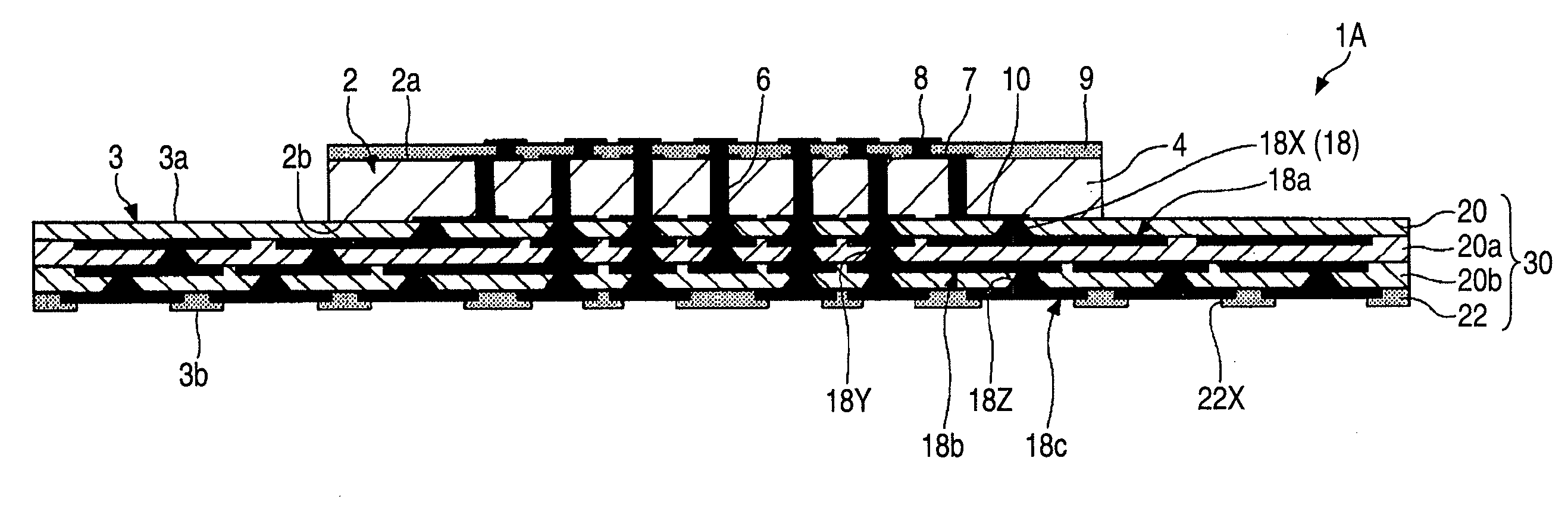
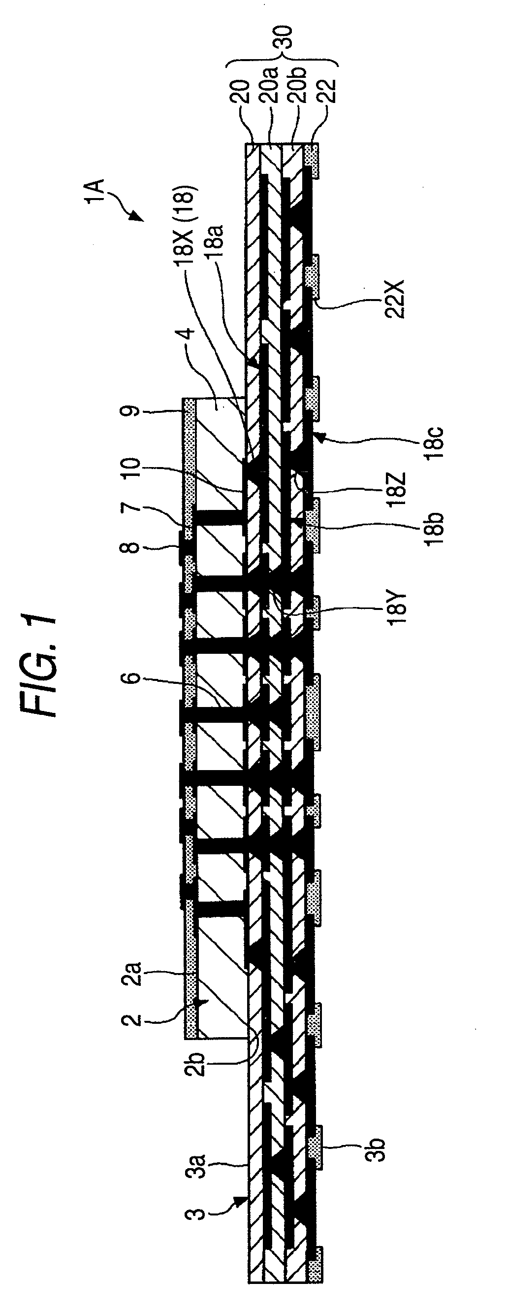
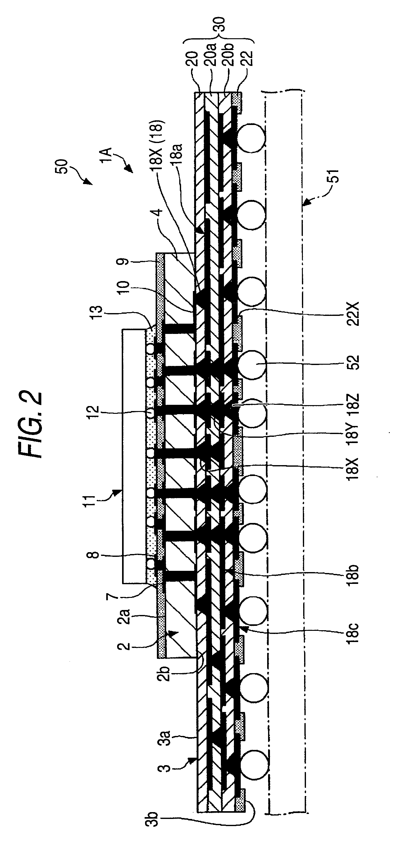
[0046]FIG. 1 shows a wiring board 1A according to an exemplary embodiment of the present invention. FIG. 2 shows a semiconductor device 50 having the wiring board 1A. The wiring board 1A, if roughly classified, includes a first board 2 and a second board 3. The first board 2 and the second board 3 are mounted.

[0047]The first board 2 is a silicon interposer and is a rectangular board having a size of 20 mm×20 mm, for example, when viewed from the top. In the exemplary embodiment, an example using the silicon interposer as the first board 2 will be described, but an organic substrate or a ceramic substrate can also be used in place of the silicon interposer if high processing accuracy can be performed.

[0048]The first board 2 includes a silicon substrate 4, through electrodes 6, upper wirings 7, chip connection pads 8, via connection pads 10, or the like.

[0049]The through e...


PUM

PropertyMeasurementUnit
sizeaaaaaaaaaa
sizeaaaaaaaaaa
thicknessaaaaaaaaaa

Abstract

The present disclosure relates to a method of manufacturing a wiring board. The method includes: (a) preparing a first board having a pad; (b) providing an insulating member on the first board, wherein a size of the insulating member is larger than that of the first board, when viewed from the top; (c) forming a via in the insulating member such that the via is directly connected to the pad; and (d) repeatedly forming a wiring layer and an insulating layer on the insulating member in which the via is formed, thereby forming a second board.

Description

[0001]This application claims priority from Japanese Patent Application No. 2007-302994, filed on Nov. 22, 2007, the entire contents of which are incorporated by reference herein.BACKGROUND[0002]1. Technical Field[0003]The present disclosure relates to a wiring board, a semiconductor device having the wiring board, and a method of manufacturing the wiring board. More particularly, the present disclosure relates to a wiring board in which a first board and a second board are built-up, a semiconductor device having the wiring board, and a method of manufacturing the wiring board.[0004]2. Related Art[0005]In recent years, with a high density semiconductor device, a wiring board mounted on the semiconductor device has also been subjected to finer design rules and high density design rules. FIG. 11 shows a wiring board that deals with the high density semiconductor device in the related art.[0006]The wiring board shown in FIG. 11 is a build-up board 100. In the build-up board 100, build-...

Claims


Application Information

Patent Timeline
Patent Type & Authority Applications(United States)
IPC IPC(8): H05K3/00
CPCH01L21/4846Y10T156/10H01L23/49816H01L23/49822H01L23/49833H01L2224/16225H01L2924/01046H01L2924/01078H01L2924/01079H01L2924/15311H01L2924/15312H05K1/112H05K3/4602H05K3/4694H05K2201/09845H05K2201/10674H05K2203/061H01L2224/32225H01L2224/73204H01L23/49811Y10T29/49126H01L2224/16235H01L2924/00H05K1/14H05K3/40H05K3/46
Inventor TANAKA, MASATOHAYANO, FUMIHIKOHIZUME, TORU
Owner SHINKO ELECTRIC IND CO LTD
Why Eureka
Try Eureka