Fullchip functional equivalency and physical verification

a functional equivalency and physical verification technology, applied in the field of semiconductor device manufacturing, can solve the problems of creating a need to backannotate information into rtl, creating a vast difference a mismatch between rtl and the layout, so as to maintain symbolic connectivity

Active Publication Date: 2008-07-22
ORACLE INT CORP
View PDF8 Cites 12 Cited by
  • Summary
  • Abstract
  • Description
  • Claims
  • Application Information

AI Technical Summary

Benefits of technology

[0008]In one embodiment of the invention, a method provides consistent rules and specifications to back-end tools and flows to update the layout and symbolic connectivity in parallel. Each tool and flow can effectively modify the layout and the schematic derived from the reference RTL. When a reference schematic does not exist, the method provides a way to use existing design verification tools to check consistency between a layout, symbolic connectivity derived netlist, and a reference RTL. The method allows at various stages in the design process to determine physical equivalency between a layout and a symbolic connectivity derived netlist, and functional equivalency between a symbolic connectivity derived netlist and a reference RTL. One embodiment allows the designer to build a full-chip netlist, check equivalency at various design levels (CPU, block levels, etc.) and use the same netlist for full-chip or mixed-mode physical layout versus schematic verification.
[0010]In one embodiment, the invention relates to a method for maintaining symbolic connectivity in an integrated circuit design which includes providing a reference Register Transfer Logic (RTL) design representation of the integrated circuit design, generating a netlist representation of the integrated circuit design, generating a physical layout of the integrated circuit design based upon the netlist representation of the integrated circuit design, and maintaining equivalency between the reference RTL design and a physical layout design of the integrated circuit design via the netlist representation of the integrated circuit design.

Problems solved by technology

In an aggressive integration methodology, the modification of logic represented by the layout due to placement, route topologies, and clock loading constraints can create a mismatch between RTL and the layout.
However, these approaches can create a vast difference between the RTL and corresponding layout, and create a need to back-annotate information into RTL.

Method used


Image

  • Fullchip functional equivalency and physical verification
  • Fullchip functional equivalency and physical verification
  • Fullchip functional equivalency and physical verification

Examples


Embodiment Construction

[0018]The present invention and its various embodiments provide an apparatus and method to achieve equivalency for all designs that use symbolic routing at the top level.

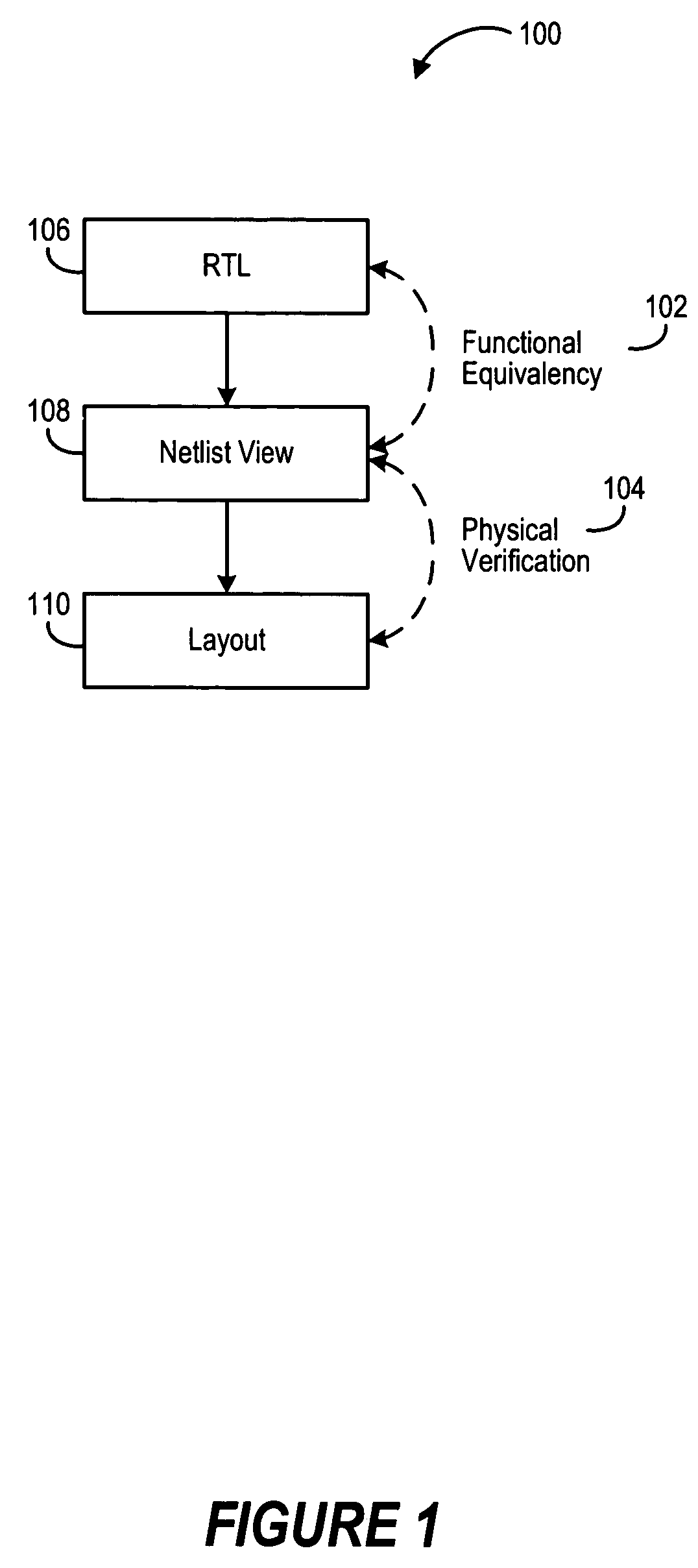
[0019]Referring to FIG. 1, a block diagram of an equivalency operation 100, used for broad level checks between register transfer level (RTL) 106 and a layout 110, is shown. In this embodiment, the method is performed in two steps. In step 102, functional equivalency is checked between RTL 106 and netlist view 108. In step 104 netlist view 108 and layout 110 are compared and physically verified using a layout versus schematic (LVS) procedure. In this embodiment of the invention, netlist view 108 is the common link and ensures consistency through the operations at steps 102 and 104.

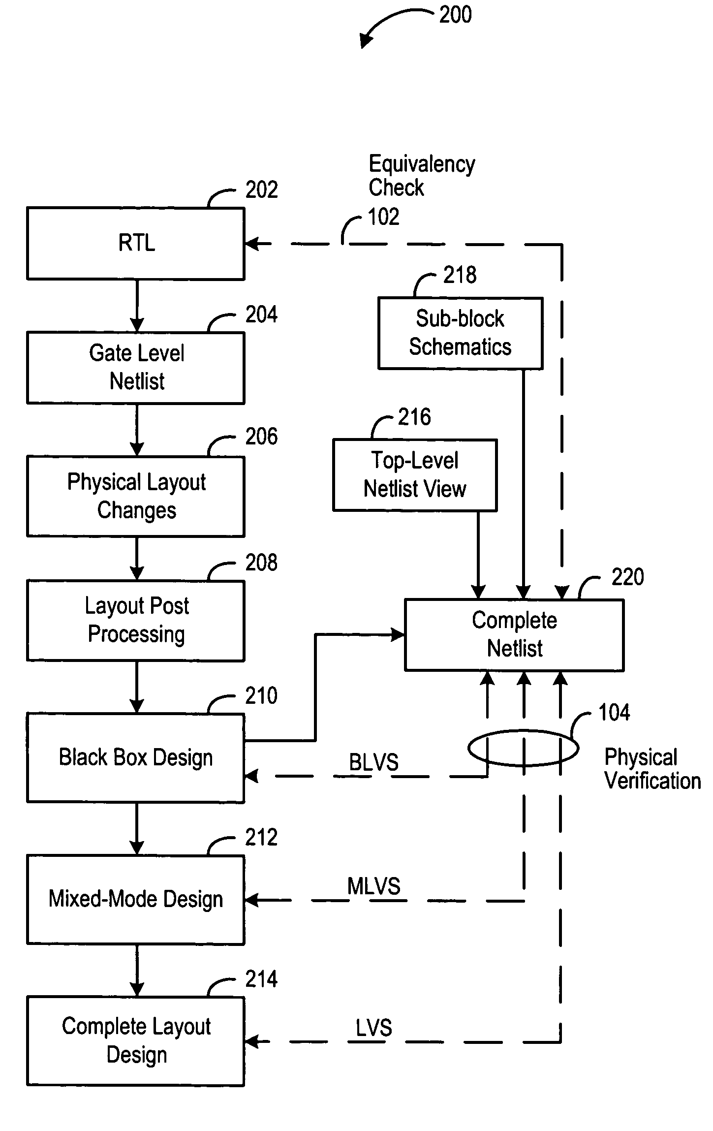
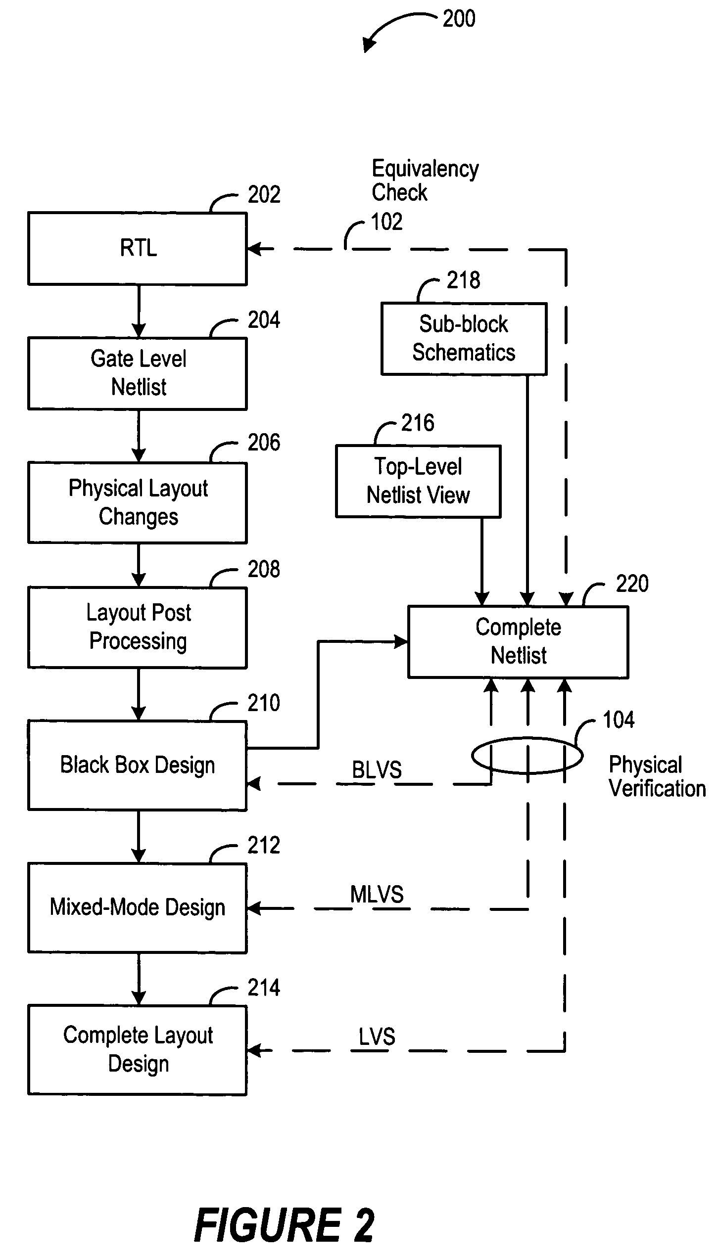
[0020]Referring to FIG. 2, an embodiment of the equivalency operation 100 is shown in a flowchart illustrating the operation of a system 200 for performing physical verification and functional equivalency checking. More specifically, at st...


PUM


Abstract

A method for maintaining equivalency between the reference Register Transfer Logic (RTL) and the physical layout design of an integrated circuit by way of maintaining a reference netlist derived from symbolic connectivity.

Description

BACKGROUND OF THE INVENTION[0001]1. Field of the Invention[0002]The present invention relates to semiconductor device manufacturing, and more particularly, maintaining equivalency between a logical design and a physical design of an integrated circuit.[0003]2. Description of the Related Art[0004]Integrated circuits (IC), such as application specific integrated circuits (ASIC), are typically designed using computer-aided design (CAD) tools using a hardware description language (HDL) that allow the designer to specify, in software, the logical operation of the chip. One such example of a hardware description language is Verilog.[0005]Known design processes include several steps. First, a designer writes a software program describing the flow of signals in the chip and the logical operations performed on those signals. In Verilog, for example, such a program is written at the Register Transfer Level (RTL). Once the designer has programmed the operation of the logic circuit, the program...

Claims


Application Information

Patent Timeline
Patent Type & Authority Patents(United States)
IPC IPC(8): G06F17/50
CPCG06F17/5068G06F17/5045G06F30/39G06F30/30G06F30/398
Inventor DUTT, ARJUNHOEROLD, STEPHAN
Owner ORACLE INT CORP
Why Eureka
Try Eureka