Wafer stack, integrated optical device and method for fabricating the same

a technology of optical devices and wafers, applied in the field of integrated optical devices, can solve the problems of reduced image quality, known modules and manufacturing processes, artifacts in images, etc., and achieve the effect of low cos

Active Publication Date: 2011-01-20
AMS SENSORS SINGAPORE PTE LTD
View PDF6 Cites 43 Cited by
  • Summary
  • Abstract
  • Description
  • Claims
  • Application Information

AI Technical Summary

Benefits of technology

[0017]It is a further object of the invention to provide an integrated optical device that can be manufactured in a mass production process at low cost, and a corresponding manufacturing process.

Problems solved by technology

This may lead to artifacts in the image generated by the image capturing element, and thus to a reduced image quality.
The additional steps of attaching each individual baffle to each individual camera module associated therewith is time-consuming and complicated and, thus, another disadvantage of known modules and manufacturing processes.
A further disadvantage is that the optical system, or at least the top lens element or the iris layer, is fully accessible via the through hole.
This may lead to damage and contamination.

Method used


Image

  • Wafer stack, integrated optical device and method for fabricating the same
  • Wafer stack, integrated optical device and method for fabricating the same

Examples


Embodiment Construction

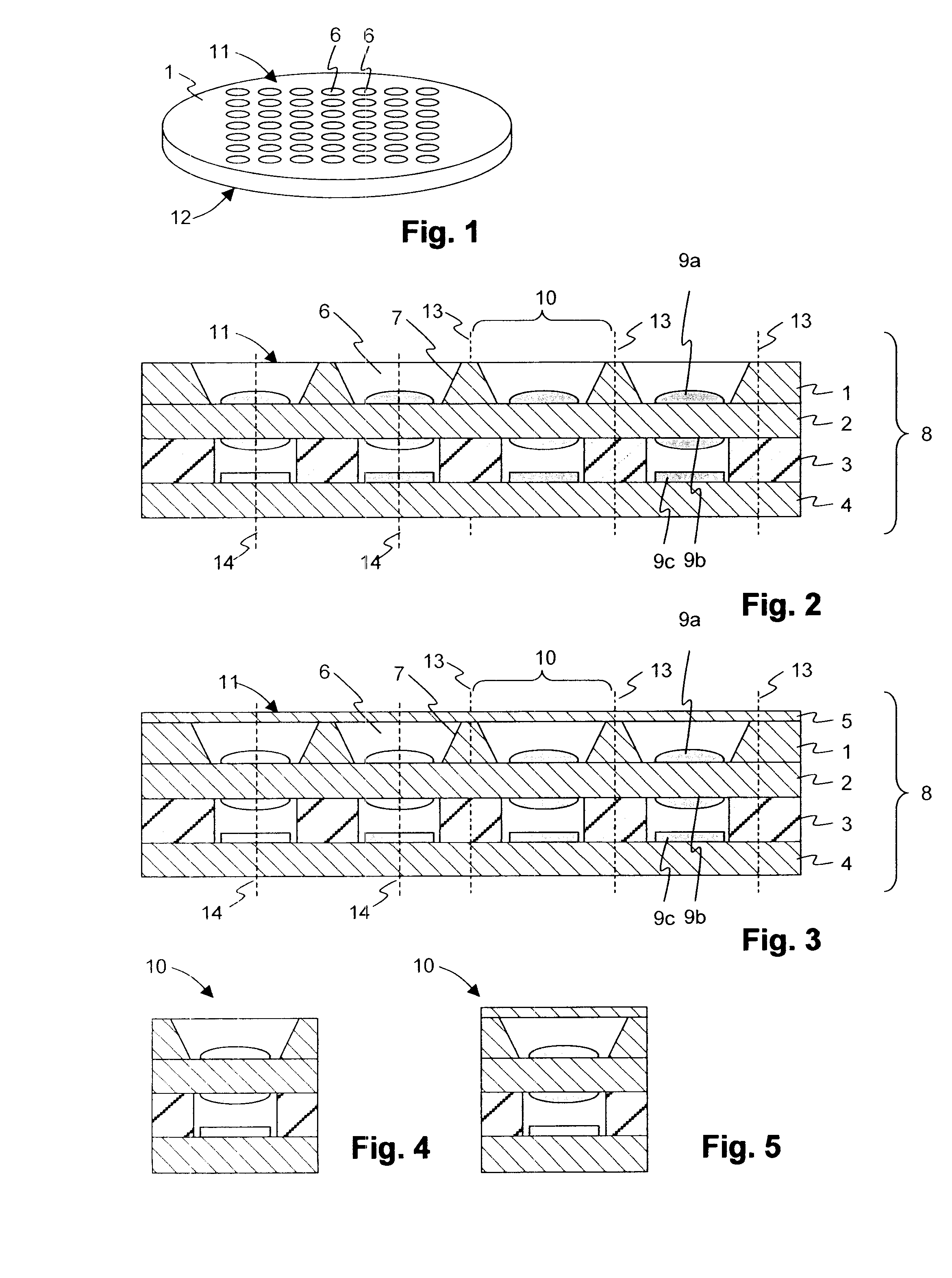
[0034]FIG. 1 schematically shows an elevated view of a sunshade plate. The sunshade plate 1 is wafer-sized and comprises a plurality of through holes 6, typically arranged in a grid or array. The through holes 6 extend from a top surface 11 to a bottom surface 12 of the sunshade plate 1 and preferably are conical in shape.

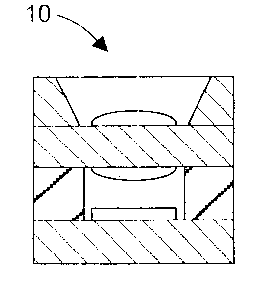
[0035]FIGS. 2 and 3 show lateral cut-away views of wafer stacks 8 with a sunshade plate 1. A wafer stack 8 comprises, from top to bottom, a sunshade plate 1 stacked on a top wafer 2 carrying functional elements, for example, a first lens 9a and second lens 9b. Alternatively, the top wafer 2 may carry only lenses on its top or only on its bottom surface. The lenses may be fabricated on the top wafer 2 by means of a replication process, or may be shaped into the top wafer 2 itself. The top wafer 2 is stacked on a further wafer 4 from which it may be separated by a spacer wafer 3. The further wafer 4 carries, as further functional elements, imaging or camera chips 9c....


PUM

PropertyMeasurementUnit
angleaaaaaaaaaa
thicknessaaaaaaaaaa
diameteraaaaaaaaaa

Abstract

In a method for fabricating an integrated optical device by creating a wafer stack by stacking at least a top wafer carrying as functional elements a plurality of lenses on at least one further wafer including further functional elements, and separating the wafer stack into a plurality of integrated optical devices, wherein corresponding functional elements of the top and further wafer are aligned with each other and define a plurality of main optical axes, a method for providing a sunshade plate as part of an integrated optical device (10), including the steps of: providing a sunshade plate having a plurality of through holes, the through holes being arranged to correspond to the arrangement of the functional elements on the top wafer; and stacking the sunshade plate on the top wafer, with the through holes being aligned with said main optical axes.

Description

BACKGROUND OF THE INVENTION[0001]b 1. Field of the Invention[0002]The invention is in the field of integrated optical devices, in particular integrated camera modules with an image capturing element, such as a CCD sensor, and at least one lens element for imaging an object on the image capturing element, e.g. a refractive and / or diffractive lens. Integrated device means that all components are arranged in a well defined spatial relationship. Such integrated camera modules are, for example, cameras of mobile phones which are preferably manufactured in a mass production process at low cost.[0003]More concretely, the invention relates to an optical device for a camera module comprising a baffle that defines a predetermined field of view (FOV) of the image capturing device, while suppressing beam paths coming from points outside this FOV. The invention further relates to a wafer scale package representing a plurality of such optical devices, to a baffle array with a plurality of baffles...

Claims


Application Information

Patent Timeline
Patent Type & Authority Applications(United States)
IPC IPC(8): G02B3/00G02B5/00B23P11/00
CPCH01L27/14621Y10T29/49826H01L31/02164H01L27/14685
Inventor ROSSI, MARKUSRUDMANN, HARTMUT
Owner AMS SENSORS SINGAPORE PTE LTD
Why Eureka
Try Eureka