Semiconductor device

Active Publication Date: 2011-01-27
SANKEN ELECTRIC CO LTD
View PDF4 Cites 2 Cited by
  • Summary
  • Abstract
  • Description
  • Claims
  • Application Information

AI Technical Summary

Benefits of technology

[0009]The present invention was invented to solve the above described problems and provides a semiconductor device have a simple structure and simplified manufacturing process which can improve resistance.
[0016]In the semiconductor device related to a feature of an embodiment of the present invention, by making the width between an interior side electrical field buffer region and a width of an exterior side electrical field buffer region different, it is possible to accelerate a widening of an exterior side depletion layer and buffer an electrical field. In this way, it is possible to improve resistance of the semiconductor device. As a result, in the semiconductor device, it is possible to make the shape of the first columnar region and the second columnar region the same and because it is possible to easily adjust the amount of impurities in the first columnar reign and the second columnar region it is possible to simplify the manufacturing process.

Problems solved by technology

However, in the technology disclosed in patent document 1, there is the problem that the manufacturing process becomes complex because the depth and width of columnar regions are different.
In particular, when the depth of columnar regions is different, it is difficult to make the amount of purities in each columnar region equal and it is very difficult to adjust the amount of implanted ions.

Method used


Image

  • Semiconductor device
  • Semiconductor device
  • Semiconductor device

Examples


Embodiment Construction

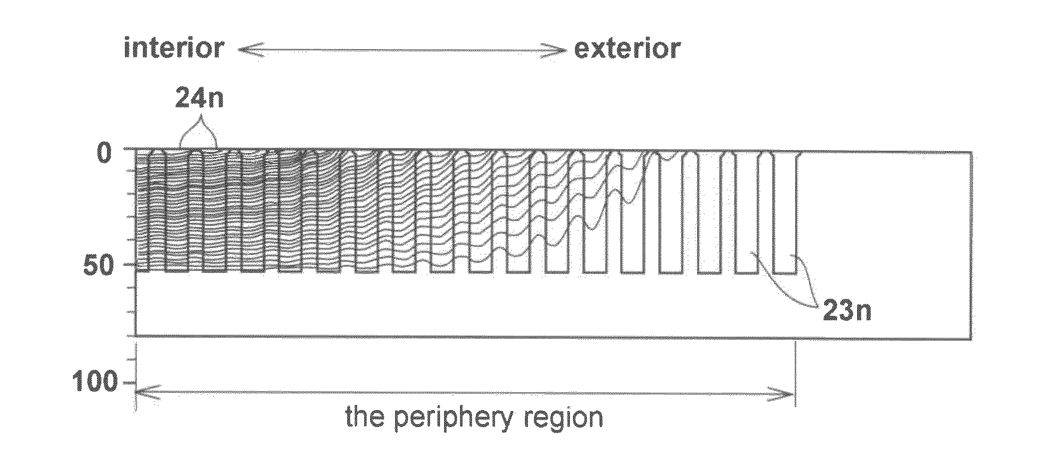
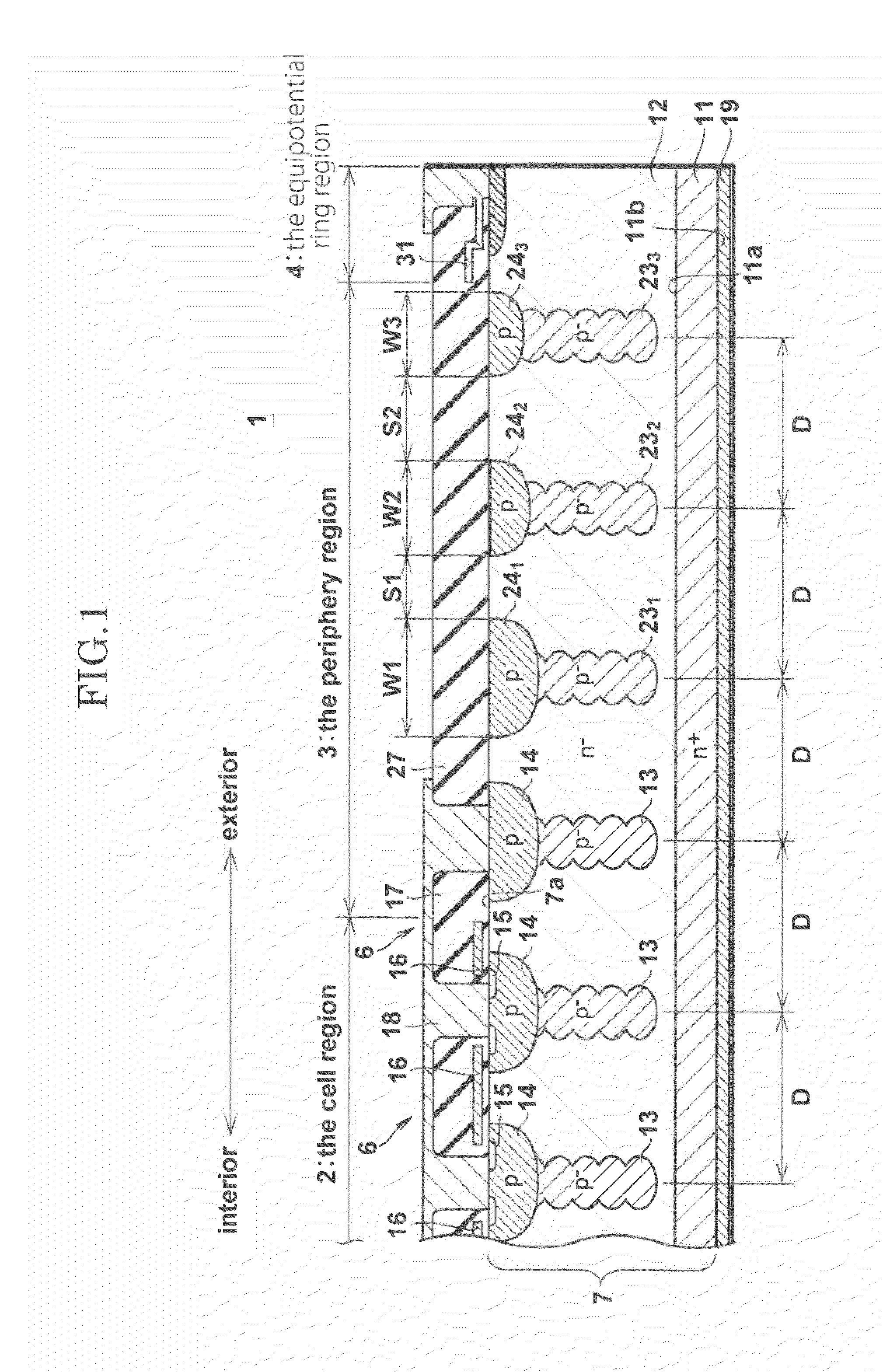
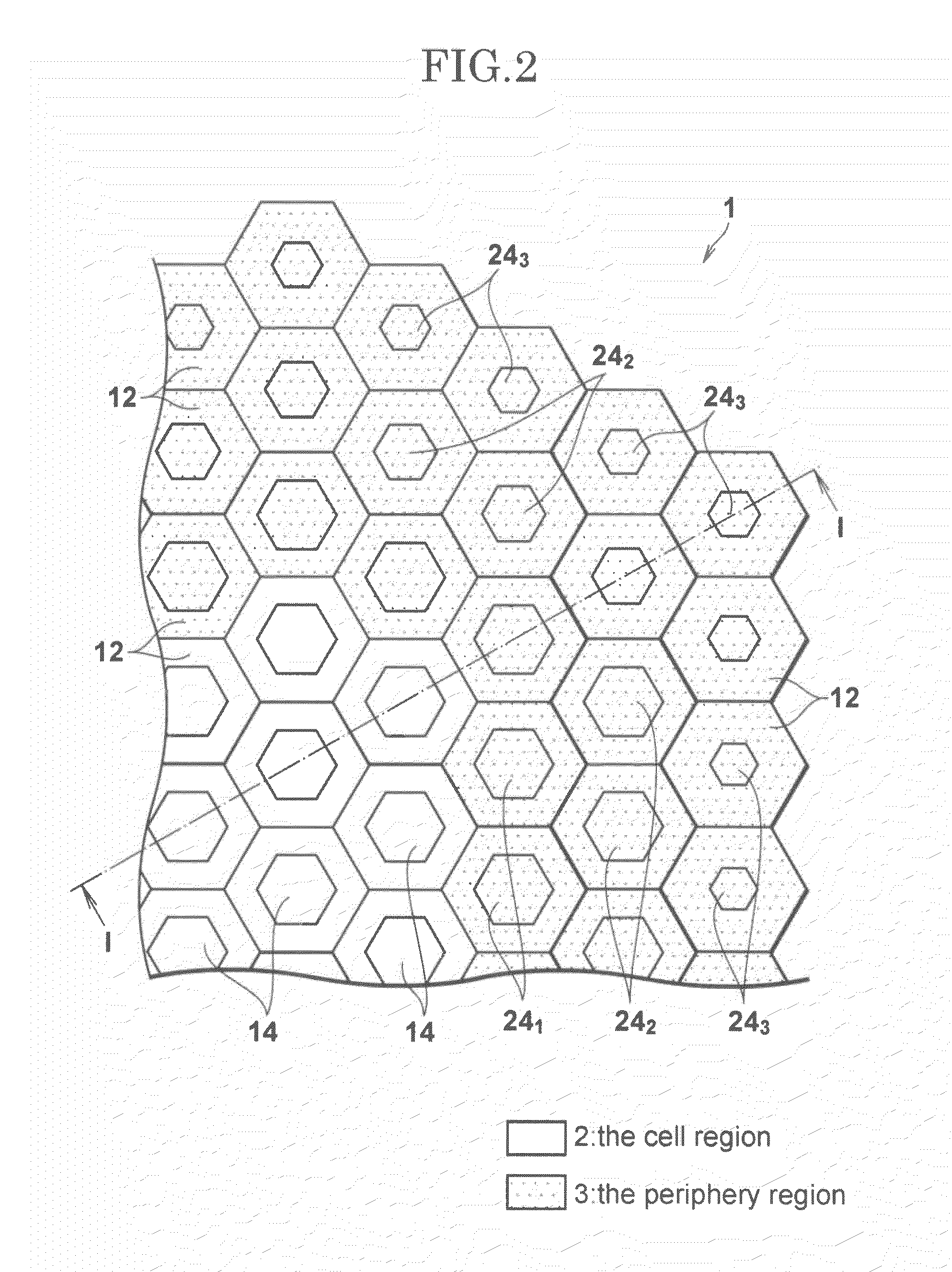
[0029]A embodiment in which the present invention is applied to a semiconductor device having a plurality of FET (field effect transistor) is explained below while referring to the diagrams. Here, FIG. 1 is a cross sectional diagram of a semiconductor device related to the present embodiment. FIG. 2 is a planar abbreviated diagram of the semiconductor device. Furthermore, the cross sectional diagram shown in FIG. 1 is a cross sectional view along the line I-I shown in FIG. 2. In the explanation below, [exterior] and [interior] indicated by arrows in FIG. 1, indicate the [exterior side] and [interior side] of the semiconductor device. The planar abbreviated diagram shown in FIG. 2 is a diagram in which the characteristic structure has been extracted and depicted in order to easily explain the flat shape of a p type base region and an electric filed buffer region. Unrelated structure is omitted from this explanation.

[Structure of the Semiconductor Device]

[0030]As is shown in FIG. 1 an...


PUM


Abstract

A semiconductor device 1 including a cell region 2 formed with a semiconductor element 6 and a periphery region 3 formed in the periphery of the cell region 2. The semiconductor region 1 is arranged with an n− type drift region 12 formed in the cell region 2 and periphery region 3, a plurality of p− type columnar regions formed in the n− drift region 12 of the cell region 2, a plurality of p− type columnar resistance improvement regions 23n formed in the n− type drift region 12 of the periphery region 3, and a plurality of electrical field buffer regions 24n formed in an upper part of the p− type columnar region 23n. An interval Sn between the electrical field buffer region 24n and an adjacent electrical field buffer region 24n is different between an interior side and an exterior side of the periphery region 3.

Description

CROSS REFERENCE TO RELATED APPLICATION[0001]This application is based upon and claims the benefit of priority from the prior Japanese Patent Application No. 2009-173268 filed on Jul. 24, 2009, the entire contents of which is incorporated herein by reference.BACKGROUND OF THE INVENTION[0002]1. Field of the Invention[0003]The present invention is related to a semiconductor device and in particular, a semiconductor device having a super junction which includes a columnar region which extends in the thickness direction of a substrate.[0004]2. Description of the Related Art[0005]A semiconductor device having a super junction structure is conventionally known. In patent document 1 (Japan Laid Open Patent 2006-5275), a semiconductor device is disclosed having a super junction structure arranged with a cell region formed with a plurality of semiconductor elements and a periphery region for resistance improvement. In a cell region of this semiconductor device, a plurality of first p type col...

Claims


Application Information

Patent Timeline
IPC IPC(8): H01L29/06
CPCH01L29/0619H01L29/0634H01L29/7811H01L29/1095H01L29/66712H01L29/0638
Inventor OMORI, TOMOYUKI
Owner SANKEN ELECTRIC CO LTD
Why Eureka
Try Eureka