High-bandwidth ramp-stack chip package

Active Publication Date: 2011-01-27
ORACLE INT CORP
View PDF44 Cites 22 Cited by
  • Summary
  • Abstract
  • Description
  • Claims
  • Application Information

AI Technical Summary

Benefits of technology

[0015]Note that the ramp component may be mechanically coupled to the semiconductor dies without inserting the semiconductor dies into slots in the ramp component. In some em

Problems solved by technology

However, TSVs typically have a higher cost than wire bonds.
This opportunity cost can be large.
(In fact, the overhead is likely to be even larger because circuits are typical

Method used


Image

  • High-bandwidth ramp-stack chip package
  • High-bandwidth ramp-stack chip package
  • High-bandwidth ramp-stack chip package

Examples


Embodiment Construction

[0036]The following description is presented to enable any person skilled in the art to make and use the disclosure, and is provided in the context of a particular application and its requirements. Various modifications to the disclosed embodiments will be readily apparent to those skilled in the art, and the general principles defined herein may be applied to other embodiments and applications without departing from the spirit and scope of the present disclosure. Thus, the present disclosure is not intended to be limited to the embodiments shown, but is to be accorded the widest scope consistent with the principles and features disclosed herein.

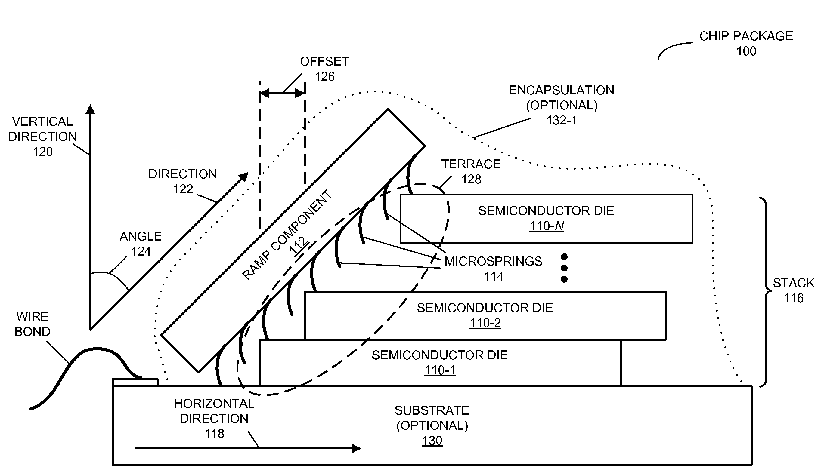
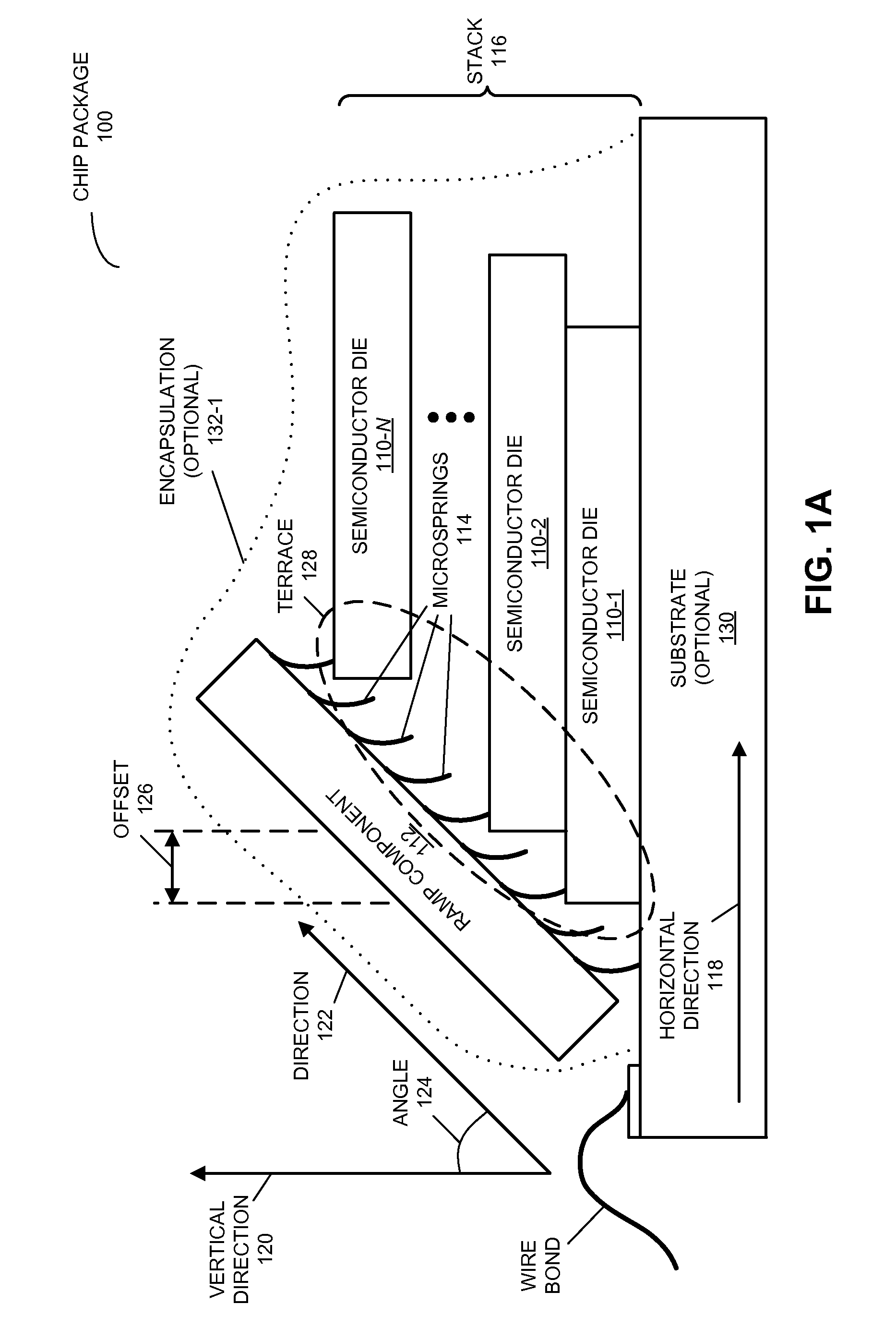
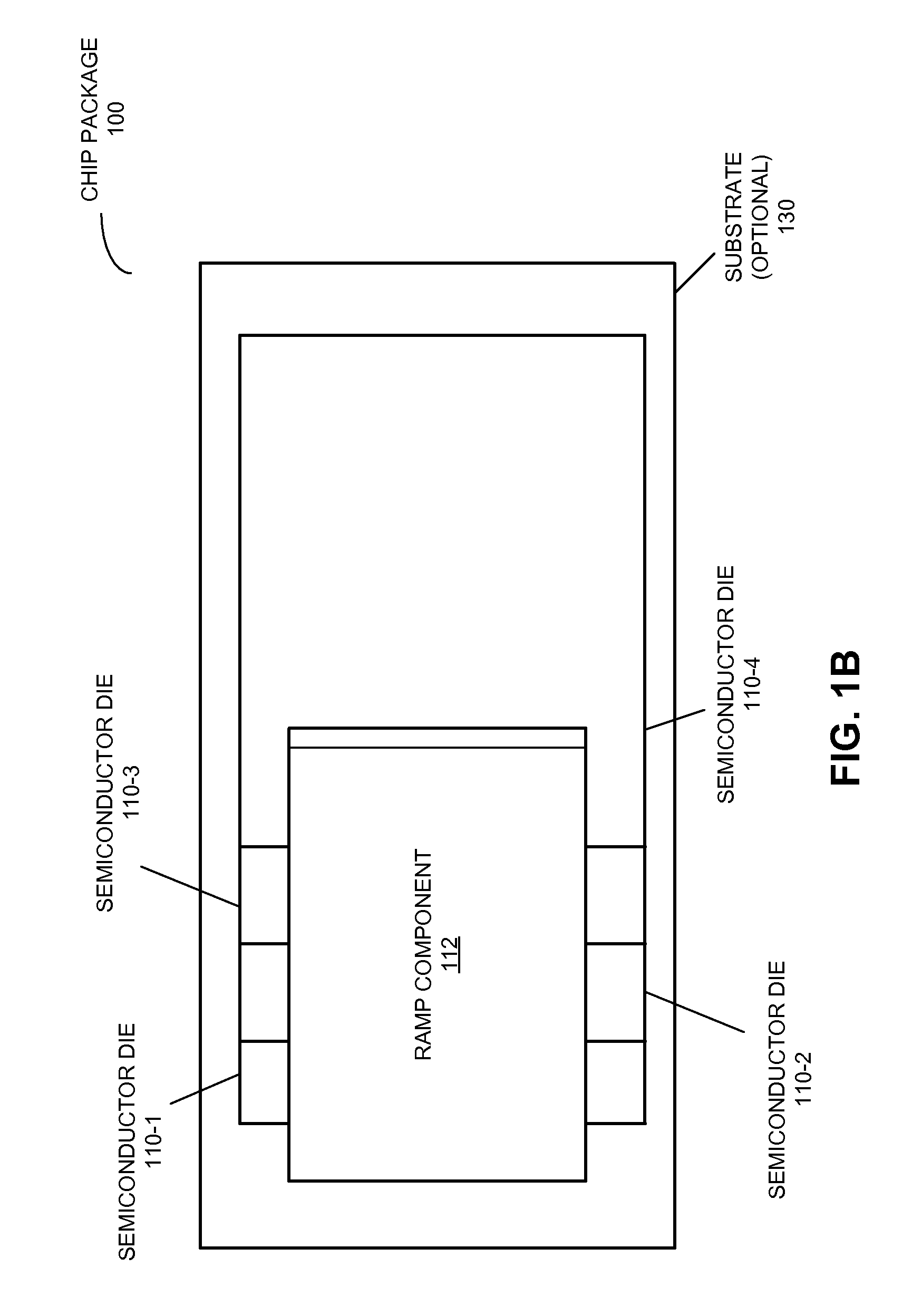
[0037]Embodiments of a chip package, an electronic device that includes the chip package, and a computer system that includes the chip package are described. This chip package includes a stack of semiconductor dies or chips that are offset from each other, thereby defining a terrace with exposed pads. A high-bandwidth ramp component, which i...


PUM


Abstract

A chip package is described. This chip package includes a stack of semiconductor dies or chips that are offset from each other, thereby defining a terrace with exposed pads. A high-bandwidth ramp component, which is positioned approximately parallel to the terrace, electrically couples to the exposed pads. For example, the ramp component may be electrically coupled to the semiconductor dies using: microsprings, an anisotropic film, and/or solder. Consequently, the electrical contacts may have a conductive, a capacitive or, in general, a complex impedance. Furthermore, the chips and/or the ramp component may be positioned relative to each other using a ball-and-pit alignment technique. By removing the need for costly and area-consuming through-silicon vias (TSVs) in the semiconductor dies, the chip package facilitates chips to be stacked in a manner that provides high bandwidth and low cost.

Description

BACKGROUND[0001]1. Field[0002]The present disclosure generally relates to a semiconductor chip package. More specifically, the present disclosure relates to a chip package that includes a group of chips arranged in a stack, and a ramp component, which is at an angle relative to the stack, and which is coupled to the chips.[0003]2. Related Art[0004]Chip packages that include stacked semiconductor chips can provide higher performance and lower cost in comparison to conventional individually packaged chips that are connected to a printed circuit board. These chip packages also provide certain advantages, such as the ability: to use different processes on different chips in the stack, to combine higher density logic and memory, and to transfer data using less power. For example, a stack of chips that implements a dynamic random access memory (DRAM) can use a high-metal-layer-count, high-performance logic process in a base chip to implement input / output (I / O) and controller functions, an...

Claims


Application Information

Patent Timeline
IPC IPC(8): H01L23/538
CPCH01L23/3121H01L23/642H01L2924/10253H01L23/645H01L24/13H01L24/14H01L24/16H01L24/48H01L24/72H01L24/90H01L25/0657H01L29/0657H01L2223/6638H01L2224/13099H01L2224/32145H01L2224/48137H01L2224/48157H01L2225/06527H01L2225/06551H01L2225/06555H01L2225/06562H01L2225/06572H01L2225/06575H01L2225/06589H01L2924/01013H01L2924/01058H01L2924/14H01L2924/1433H01L2924/15311H01L2924/19041H01L2924/19042H01L2924/19104H01L2924/19106H01L2924/19107H01L2924/30105H01L2924/30107H01L2924/3011H01L2924/01006H01L2924/01033H01L2924/01055H01L2924/01067H01L2924/014H01L2224/32225H01L2924/00H01L2924/00014H01L25/0652H01L2224/13025H01L2224/45099H01L2224/45015H01L2924/207
Inventor DROST, ROBERT J.MITCHELL, JAMES G.DOUGLAS, DAVID C.
Owner ORACLE INT CORP
Why Eureka
Try Eureka