Formation of silicon oxide using non-carbon flowable CVD processes

a technology of silicon oxide and flowable cvd, which is applied in the direction of chemical vapor deposition coating, coating, metallic material coating process, etc., can solve the problems of dielectric material, dielectric material, and structural features of the device having decreased spatial dimensions, so as to reduce the size of the gap, less shrinkage, and less pore formation

Active Publication Date: 2011-02-10
APPLIED MATERIALS INC
View PDF110 Cites 443 Cited by
  • Summary
  • Abstract
  • Description
  • Claims
  • Application Information

AI Technical Summary

Benefits of technology

Methods, materials, and systems are described for forming silicon oxide layers from flowable materials with fewer pores and less shrinkage than produced by conventional SOG techniques. The methods may include the deposition of a silicon-and-nitrogen containing film (e.g., a silic...

Problems solved by technology

The decreasing feature sizes result in structural features on the device having decreased spatial dimensions.
The widths of gaps and trenches on the device narrow to a point where the aspect ratio of gap depth to its width becomes high enough to make it challenging to fill the gap with dielectric material.
The depositing dielectric material is prone to clog at the top before the gap completely fills, producing a void or seam in the middle of ...

Method used


Image

  • Formation of silicon oxide using non-carbon flowable CVD processes
  • Formation of silicon oxide using non-carbon flowable CVD processes
  • Formation of silicon oxide using non-carbon flowable CVD processes

Examples


Embodiment Construction

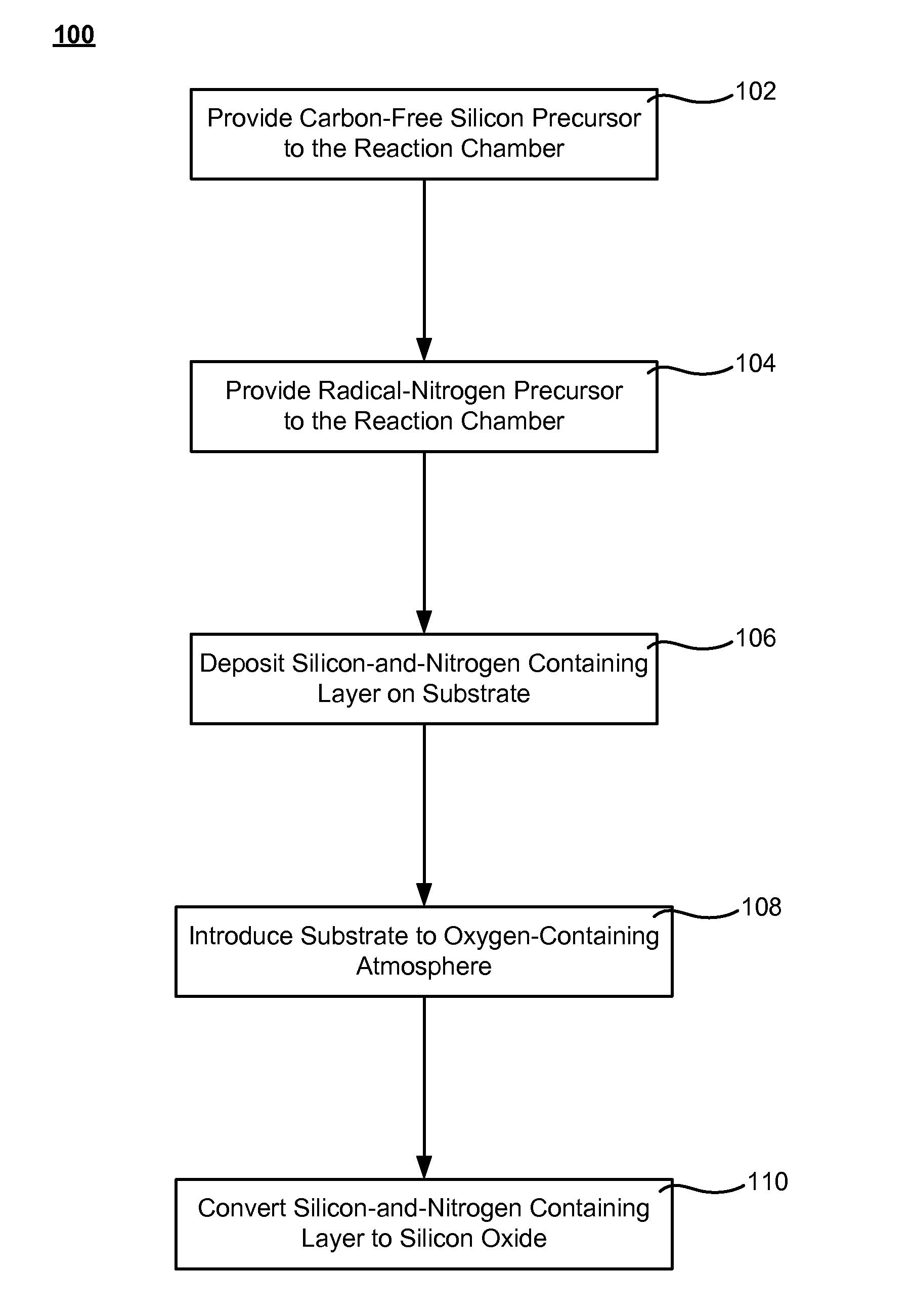
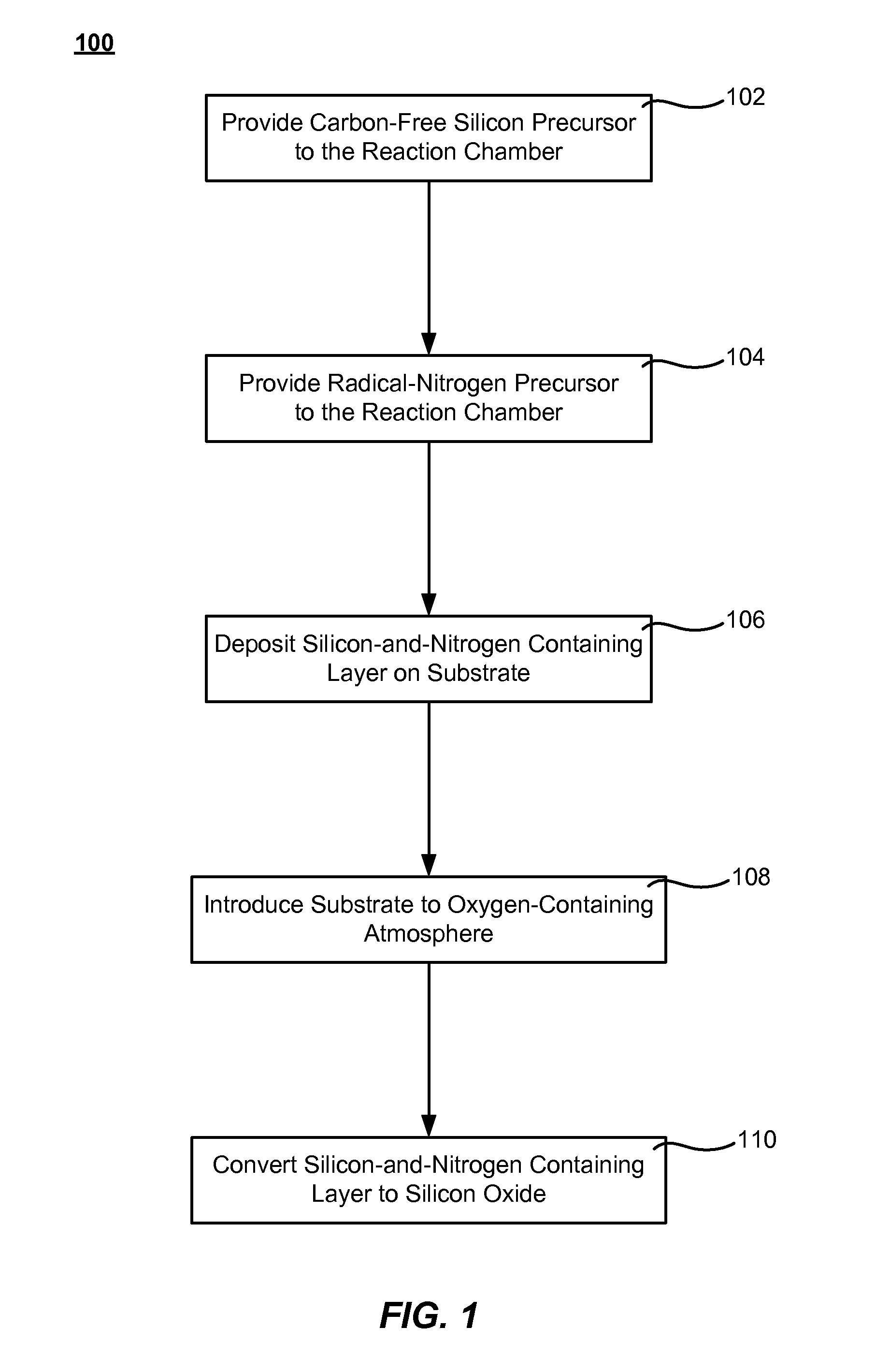
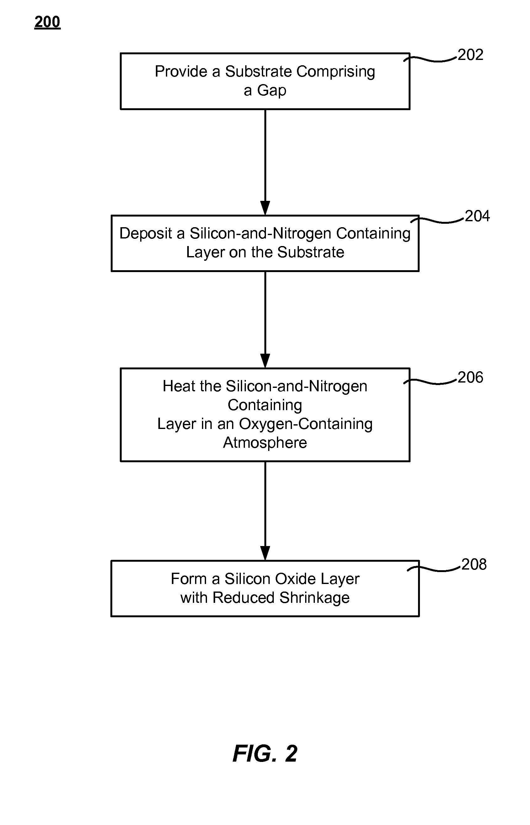
The formation of a silicon oxide layer with reduced porosity and shrinkage from a flowable silicon-and-nitrogen containing layer is described. The flowable silicon-and-nitrogen containing layer may be formed substantially free of carbon from precursors that lack carbon-containing moieties. When the substantially carbon free silicon-and-nitrogen containing layer is converted to a silicon oxide layer, the absence of carbon in the layer results is less pore formation and shrinkage of the oxide layer compared to the starting silicon-and-nitrogen containing layer. Additional details about the methods and systems of forming the silicon oxide layer will now be described.

Exemplary Silicon Oxide Formation Process

FIG. 1 is a flowchart showing selected steps in methods 100 of making silicon oxide films according to embodiments of the invention. The method 100 includes providing a carbon-free silicon precursor to a reaction chamber 102. The carbon-free silicon precursor may be, for example, a s...


PUM

PropertyMeasurementUnit
Fractionaaaaaaaaaa
Widthaaaaaaaaaa

Abstract

A method of forming a silicon oxide layer is described. The method may include the steps of mixing a carbon-free silicon-and-nitrogen containing precursor with a radical precursor, and depositing a silicon-and-nitrogen containing layer on a substrate. The silicon-and-nitrogen containing layer is then converted to the silicon oxide layer.

Description

BACKGROUND OF THE INVENTIONSemiconductor device geometries have dramatically decreased in size since their introduction several decades ago. Modern semiconductor fabrication equipment routinely produces devices with 45 nm, 32 nm, and 28 nm feature sizes, and new equipment is being developed and implemented to make devices with even smaller geometries. The decreasing feature sizes result in structural features on the device having decreased spatial dimensions. The widths of gaps and trenches on the device narrow to a point where the aspect ratio of gap depth to its width becomes high enough to make it challenging to fill the gap with dielectric material. The depositing dielectric material is prone to clog at the top before the gap completely fills, producing a void or seam in the middle of the gap.Over the years, many techniques have been developed to avoid having dielectric material clog the top of a gap, or to “heal” the void or seam that has been formed. One approach has been to s...

Claims


Application Information

Patent Timeline
IPC IPC(8): H01L21/316
CPCC23C16/401C23C16/452C23C16/56H01L21/02164H01L21/0217H01L21/02274H01L21/762H01L21/02326H01L21/02362H01L21/31608H01L21/3185H01L21/76837H01L21/02304
Inventor LIANG, JINGMEIINGLE, NITIN K.VENKATARAMAN, SHANKAR
Owner APPLIED MATERIALS INC
Why Eureka
Try Eureka