Organic light emitting display device

a light-emitting display and organic technology, applied in semiconductor devices, instruments, computing, etc., can solve problems such as uneven brightness, and achieve the effects of reducing dead space, preventing the drop of low potential pixel power supplied through the bus line, and ensuring the width of the bus lin

Active Publication Date: 2011-02-24
SAMSUNG DISPLAY CO LTD
View PDF13 Cites 46 Cited by
  • Summary
  • Abstract
  • Description
  • Claims
  • Application Information

AI Technical Summary

Benefits of technology

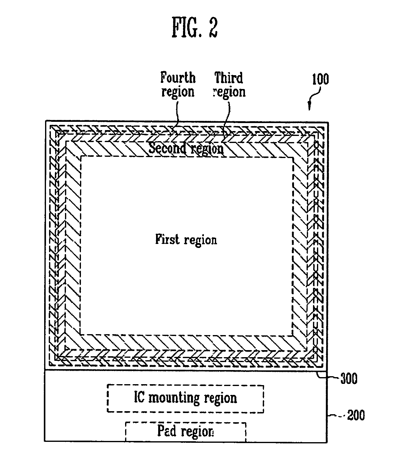
[0024]According to the embodiments, since the built-in-circuit is positioned inside the bus unit, the built-in-circuit may be prevented from being damaged by static electricity.
[0025]In addition, since the bus unit and the sealing unit overlap each other, dead space is reduced and a sufficient width of the bus lines is secured. Accordingly, IR drop of the low potential pixel power supplied through the bus lines may be prevented.

Problems solved by technology

However, brightness may not be uniform due to IR drop of the low potential pixel power.

Method used


Image

  • Organic light emitting display device
  • Organic light emitting display device
  • Organic light emitting display device

Examples


Embodiment Construction

[0030]Korean Patent Application No. 10-2009-0077045, filed on Aug. 20, 2009, in the Korean Intellectual Property Office, and entitled: “Organic Light Display Device” is incorporated by reference herein in its entirety.

[0031]In the following detailed description, only certain exemplary embodiments have been shown and described, simply by way of illustration. In the drawing figures, the dimensions of layers and regions may be exaggerated for clarity of illustration. As those skilled in the art would realize, the described embodiments may be modified in various different ways. Accordingly, the drawings and description are to be regarded as illustrative in nature and not restrictive. In addition, when an element is referred to as being “on” another element, it can be directly on another element or be indirectly on another element with one or more intervening elements interposed therebetween. It will also be understood that when a layer is referred to as being “between” two layers, it ca...


PUM


Abstract

An organic light emitting display device, comprises a pixel unit including a plurality of pixels, each of the pixels including an organic light emitting diode having a first electrode, a second electrode, and an organic light emitting layer; a built-in-circuit comprising a driving circuit configured to drive the pixels; and a bus unit comprising bus lines configured to deliver pixel power to the pixels. The pixel unit, the built-in-circuit, and the bus unit are sequentially disposed from a central region of a display panel to an outer side of the display panel. The second electrode of the organic light emitting diode and one of the bus lines are electrically connected to each other through one of conductive patterns formed on at least a part of the built-in-circuit and at least a part of the bus unit.

Description

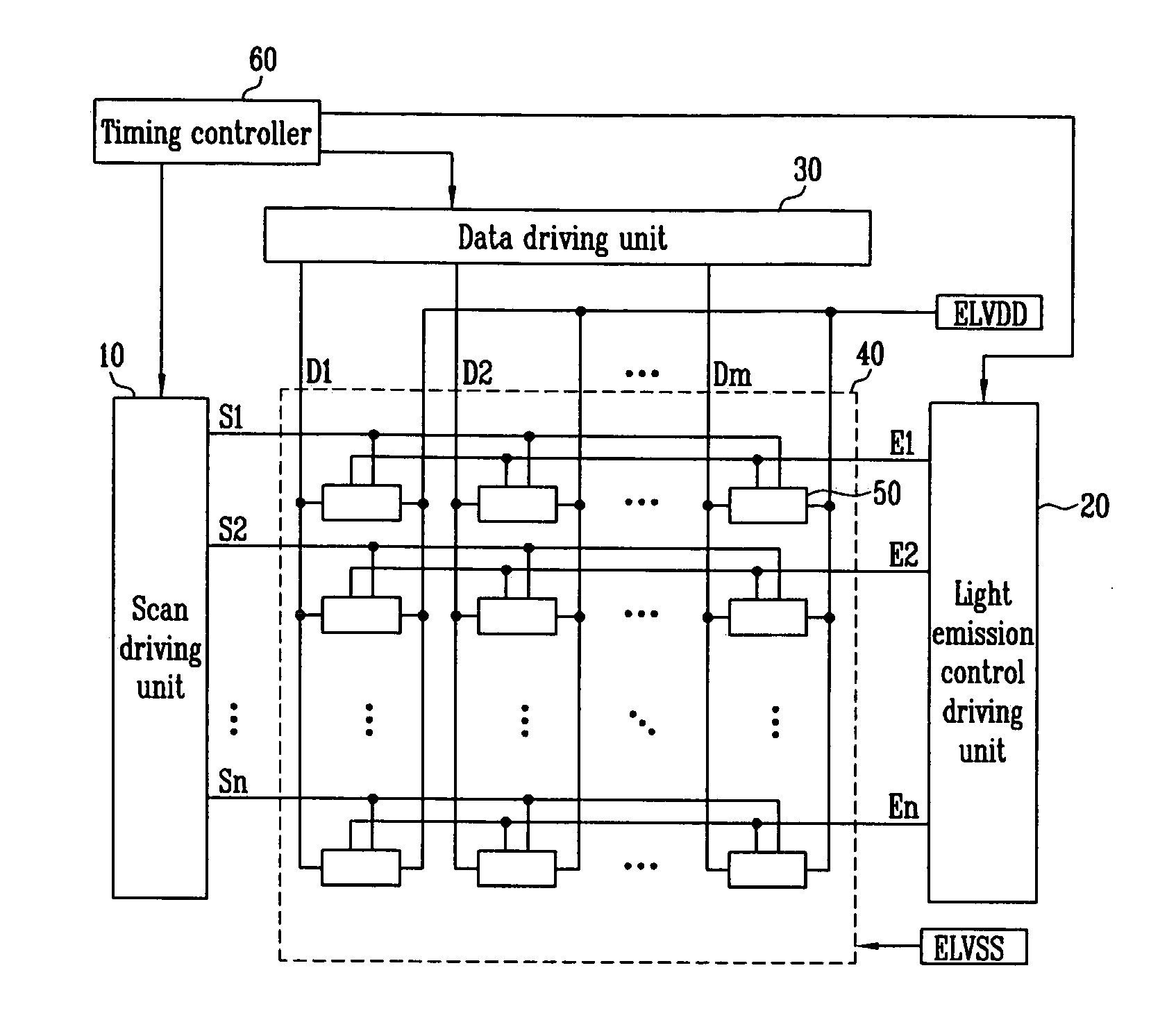
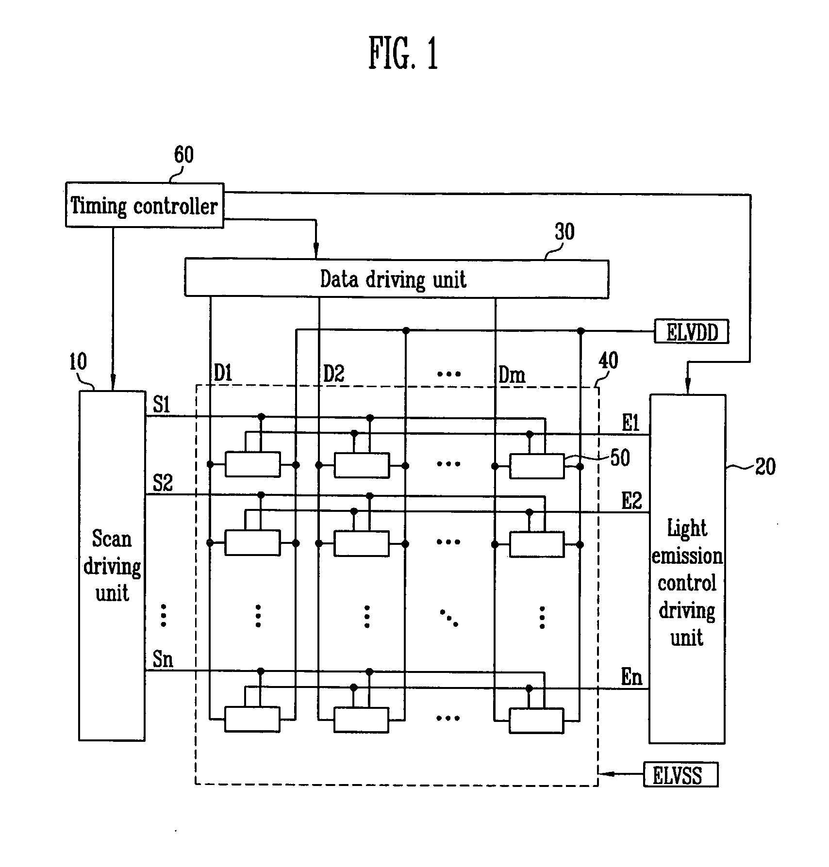
BACKGROUND[0001]1. Field[0002]The embodiments relates to an organic light emitting display device, and more particularly, to an organic light emitting display device capable of reducing dead space and preventing voltage drop of pixel power to be supplied to pixels.[0003]2. Description of the Related Art[0004]Recently, various flat panel display devices having a smaller volume of a light source than a cathode ray tube have been developed.[0005]Particularly, among the flat panel display devices, an organic light emitting display device displays an image by using organic light emitting diodes as emission devices. An organic light emitting display device attracts attention as a next generation of a display device because of its excellent brightness and color purity.[0006]An organic light emitting diode includes an anode electrode and a cathode electrode that face each other and an organic light emitting layer disposed therebetween. During emission of the organic light emitting diode, th...

Claims


Application Information

Patent Timeline
Patent Type & Authority Applications(United States)
IPC IPC(8): G09G3/30G09G5/00
CPCH01L27/3276H10K59/131H01L2027/11879H10K59/122H10K50/84H10K50/8426
Inventor BANG, HYUN-CHOLKWAK, WON-KYU
Owner SAMSUNG DISPLAY CO LTD
Why Eureka
Try Eureka