Thin Film Transistor Array Panel and Method of Manufacturing the Same

a technology of thin film transistors and array panels, which is applied in thermoelectric devices, instruments, optics, etc., can solve the problems of alignment errors, difficult to cover the edge of color filters with organic layers, and difficulty in properly aligning the two display panels

Active Publication Date: 2011-03-03
SAMSUNG DISPLAY CO LTD
View PDF3 Cites 34 Cited by
  • Summary
  • Abstract
  • Description
  • Claims
  • Application Information

AI Technical Summary

Benefits of technology

[0030]As described above, the surface height of the light blocking member is almost equal to the surface height of the organic layer such that a uniform cell gap of the liquid crystal display may be maintained. The organic layer does not remain upon forming the contact hole. The organic layer completely covers the color filter by controlling the height of the organic layer per the regions such that the contact characteristics may not be deteriorated.

Problems solved by technology

In such a liquid crystal display, the pixel electrodes and the color filters are disposed on different display panels such that it may be difficult to properly align the two display panels with each other, thereby potentially generating an alignment error.
Also, when the organic layer formed on the color filter is relatively thin, the material of the organic layer coated at the edge of the color filter tends to diffuse into a neighboring region because of the steep step shape between the color filter and the other layers make it difficult to cover the edge of the color filters with the organic layer.

Method used


Image

  • Thin Film Transistor Array Panel and Method of Manufacturing the Same
  • Thin Film Transistor Array Panel and Method of Manufacturing the Same
  • Thin Film Transistor Array Panel and Method of Manufacturing the Same

Examples


Embodiment Construction

[0039]Exemplary embodiments of the present invention will be described more fully hereinafter with reference to the accompanying drawings. The described exemplary embodiments may be modified in various different ways, all without departing from the spirit or scope of the present invention.

[0040]In the drawings, the thickness of layers, films, panels, regions, etc., may be exaggerated for clarity. Like reference numerals may designate like elements throughout the specification. It will be understood that when an element such as a layer, film, region, or substrate is referred to as being “on” another element, it can be directly on the other element or intervening elements may also be present.

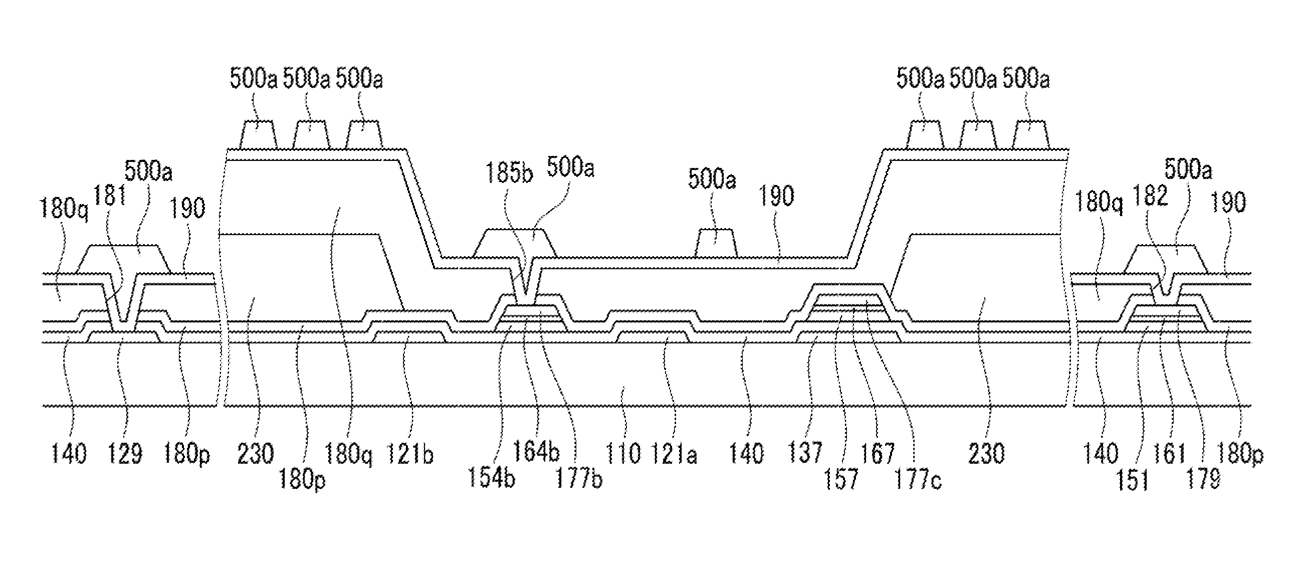
[0041]A liquid crystal display according to an exemplary embodiment of the present invention is described in detail below with reference to FIG. 1.

[0042]FIG. 1 is a schematic view of a liquid crystal display according to an exemplary embodiment of the present invention.

[0043]As shown in FIG. 1, a ...


PUM


Abstract

A thin film transistor array panel includes an insulation substrate. A signal line is formed on the insulation substrate. A thin film transistor is connected to the signal line. A color filter is formed on the substrate. An organic insulator is formed on the color filter and includes a first portion and a second portion having different thicknesses. A light blocking member is formed on the second portion of the organic insulator. A difference between the surface height of the first portion of the organic insulator and the surface height of the second portion of the organic insulator is in the range of about 2.0 μm to 3.0 μm.

Description

CROSS-REFERENCE TO RELATED APPLICATION[0001]This application claims priority to Korean Patent Application No. 10-2009-0079467 filed in the Korean Intellectual Property Office on Aug. 26, 2009, the entire contents of which are incorporated herein by reference.BACKGROUND[0002](a) Technical Field[0003]The present invention relates to thin film transistors, and more particularly, to a thin film transistor array panel and a manufacturing method thereof.[0004](b) Discussion of the Related Art[0005]Liquid crystal displays (LCDs) are one of the most widely used forms of flat panel displays. An LCD includes a pair of panels provided with field-generating electrodes and a liquid crystal (LC) layer interposed between the two panels. The LCD displays images by applying voltages to the field-generating electrodes to generate an electric field in the LC layer that determines the orientation of LC molecules therein to adjust polarization of incident light.[0006]Among the various forms of LCDs, an ...

Claims


Application Information

Patent Timeline
Patent Type & Authority Applications(United States)
IPC IPC(8): H01L33/00H01L21/28
CPCG02F1/13624G02F2001/134345H01L27/1288G02F2001/136236H01L27/1248G02F2001/136222G02F1/136236G02F1/134345G02F1/136222
Inventor KIM, JONG-INKIM, JANG-SOOYOO, HONG-SUKKIM, YONG-HWANOH, HWA-YEULCHOI, JAE-HOJANG, SANG-HEE
Owner SAMSUNG DISPLAY CO LTD
Why Eureka
Try Eureka