

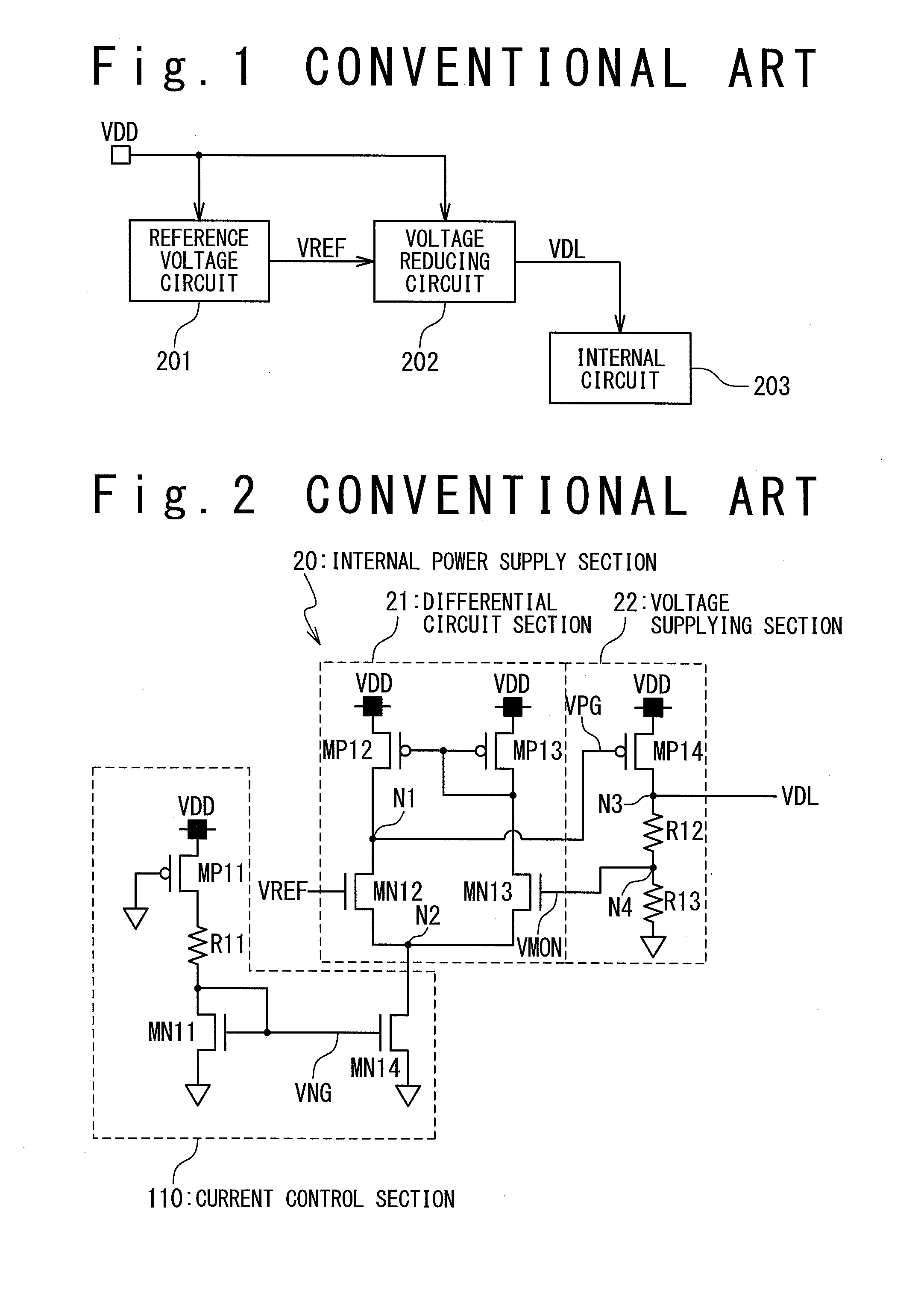
Voltage reducing circuit
a voltage reducing circuit and circuit technology, applied in the field of semiconductor devices, can solve the problems of external power supply voltage vdd and current value control section, and achieve the effect of reducing the amount of current consumption and stable operation
- Summary
- Abstract
- Description
- Claims
- Application Information
AI Technical Summary
Benefits of technology
Problems solved by technology
Method used
Image

Examples
first embodiment
[0047]FIG. 5 shows a configuration of the voltage reducing circuit according to a first embodiment of the present invention. The voltage reducing circuit in the first embodiment is applied to a semiconductor device (see FIG. 1). In this case, the voltage reducing circuit in the first embodiment corresponds to the voltage reducing circuit 202 of the semiconductor device.
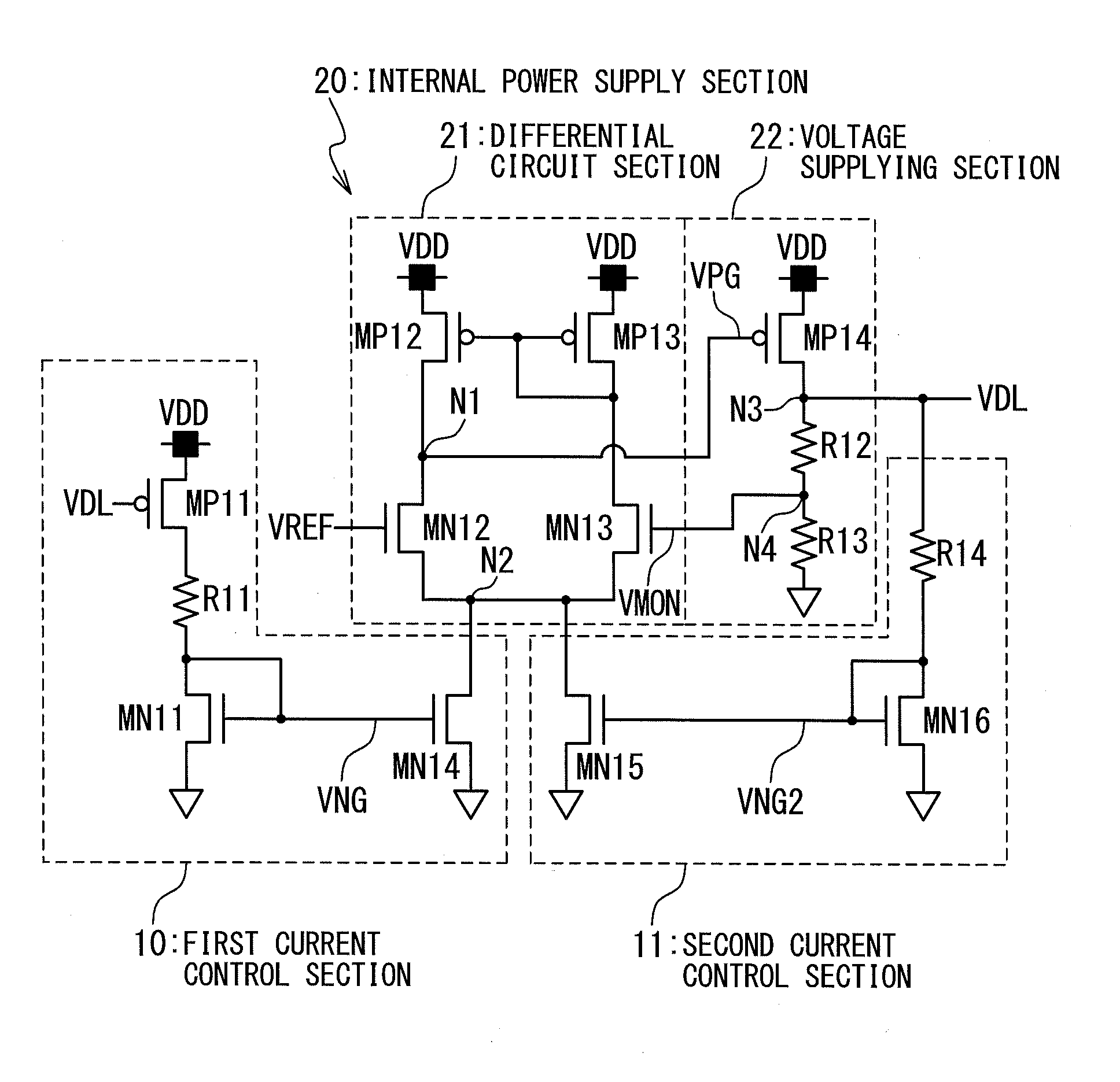
[0048]The voltage reducing circuit according to the first embodiment of the present invention includes a first current control section10, a second current control section 11, and an internal power supply section 20. The first current control section 10 includes a first P-channel MOSFET (to be referred to as a “PMOS transistor”, hereinafter) MP11, first and second N-channel MOSFETs (to be referred to as “NMOS transistors” hereinafter) MN11 and MN14, and a first resistance element R11. The second control section 11 includes third and fourth NMOS transistors MN16 and MN15 and a second resistance element R14.
[0049]The int...
second embodiment
[0067]FIG. 7 is a circuit diagram showing the configuration of the voltage reducing circuit according to a second embodiment of the present invention. In the second embodiment, a description overlapping with that of the first embodiment will be omitted.
[0068]The first current control section 10 further includes an NMOS transistor MN17. The NMOS transistor MN17 has a drain connected with a drain of the NMOS transistor MN11, a source connected with a second external power supply voltage GND, and a gate connected with a drain of the NMOS transistor MN16 of the second current control section 11.
[0069]Here, the NMOS transistor MN17 is provided in the first current control section 10, but may be provided in the second current control section 11 if the same connection relation applies.
[0070]Next, an operation of the voltage reducing circuit according to the second embodiment of the present invention will be described.
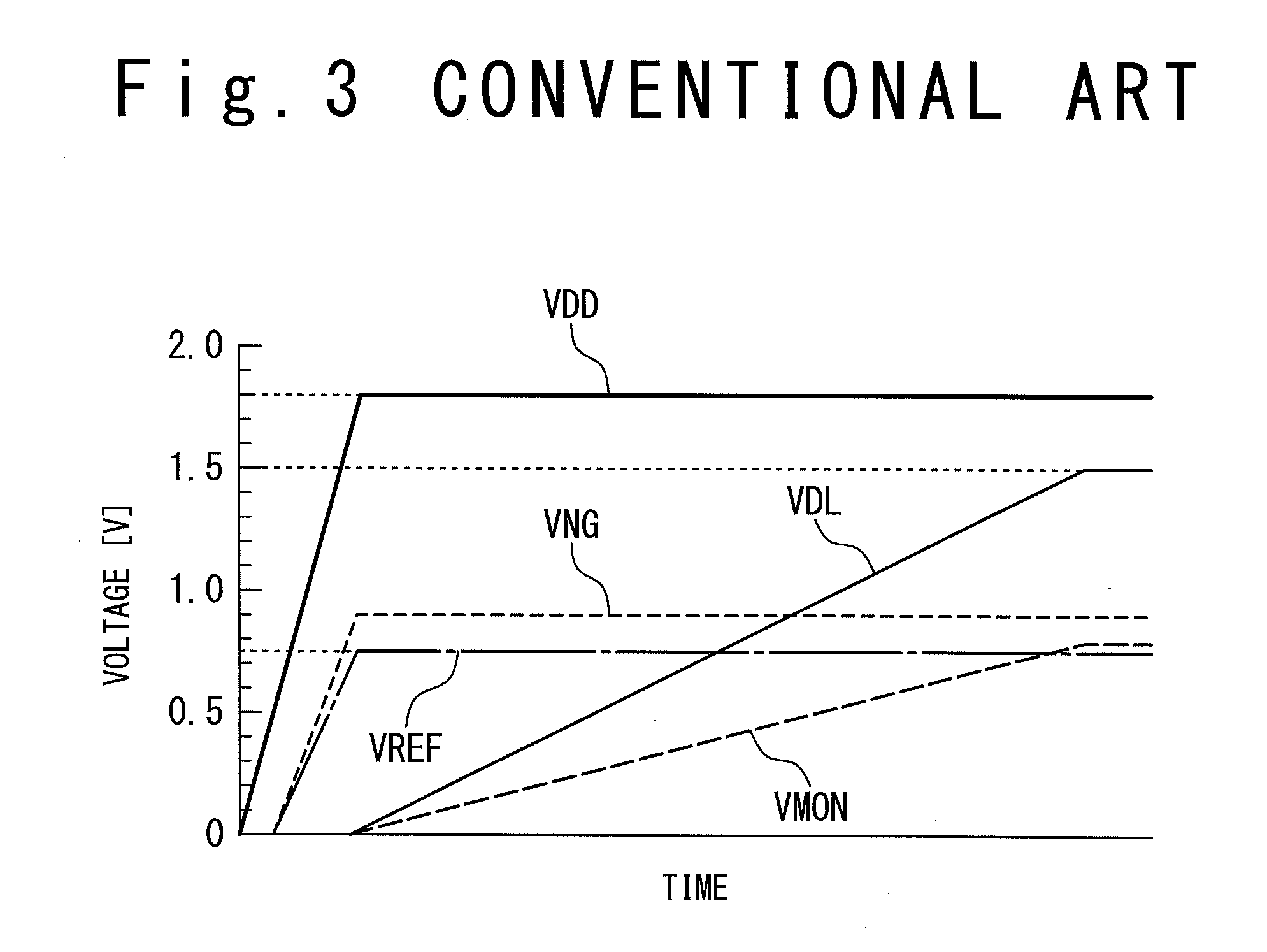
[0071]FIG. 8A illustrates time-voltage characteristics showing the operat...
PUM
 Abstract
Description
Claims
Application Information