Semiconductor integrated circuit

a technology of integrated circuits and semiconductors, applied in logic circuit coupling/interface arrangements, pulse techniques, instruments, etc., can solve the problems of inaccurate execution of data transmission between transmitters and receivers, achieve accurate transmission and reception of data, reduce power-supply noise, and execute transmission and reception accurately

Active Publication Date: 2011-03-10
RENESAS ELECTRONICS CORP
View PDF7 Cites 40 Cited by
  • Summary
  • Abstract
  • Description
  • Claims
  • Application Information

AI Technical Summary

Benefits of technology

[0013]With the circuit structure as described above, it is possible to execute transmission and reception of data accurately by reducing the power-supply noise.
[0014]According

Problems solved by technology

In a semiconductor integrated circuit, there has been a problem that data transmission between transmitter-receivers is not accu

Method used


Image

  • Semiconductor integrated circuit
  • Semiconductor integrated circuit
  • Semiconductor integrated circuit

Examples


first exemplary embodiment

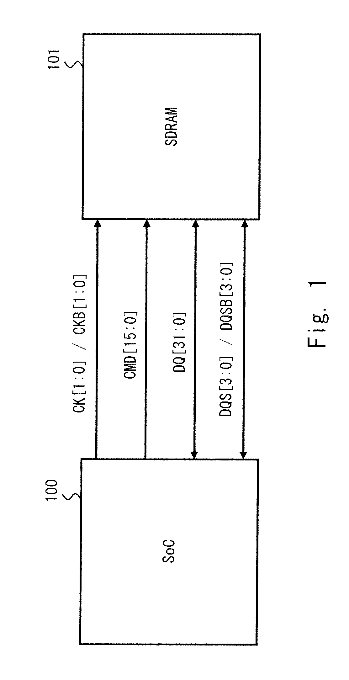
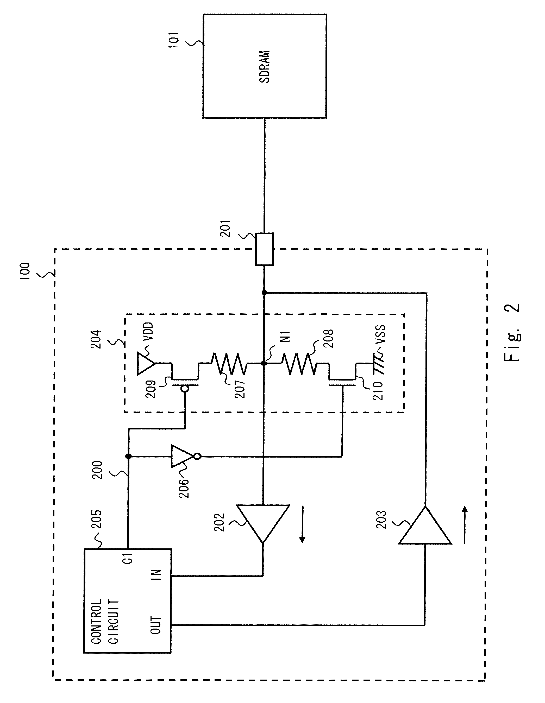
[0021]Referring to the drawings, a semiconductor integrated circuit according to a first exemplary embodiment of the present invention will be described. The present invention can be applied to a circuit which includes a first transmitter-receiver, a second transmitter-receiver, and a signal line for bidirectionally transmitting data between the first transmitter-receiver and the second transmitter-receiver (hereinafter, referred to simply as “bidirectional signal line”), and has an ODT function. In this exemplary embodiment, a case is explained hereinafter in which the circuit shown in FIG. 1 includes an SoC (System on Chip) circuit and an SDRAM (Synchronous Dynamic Random Access Memory) circuit, and data transmission is executed between the SoC circuit and the SDRAM circuit through the bidirectional signal line.

[0022]FIG. 1 illustrates a semiconductor integrated circuit according to the first exemplary embodiment of the present invention. The circuit shown in FIG. 1 includes an So...

second exemplary embodiment

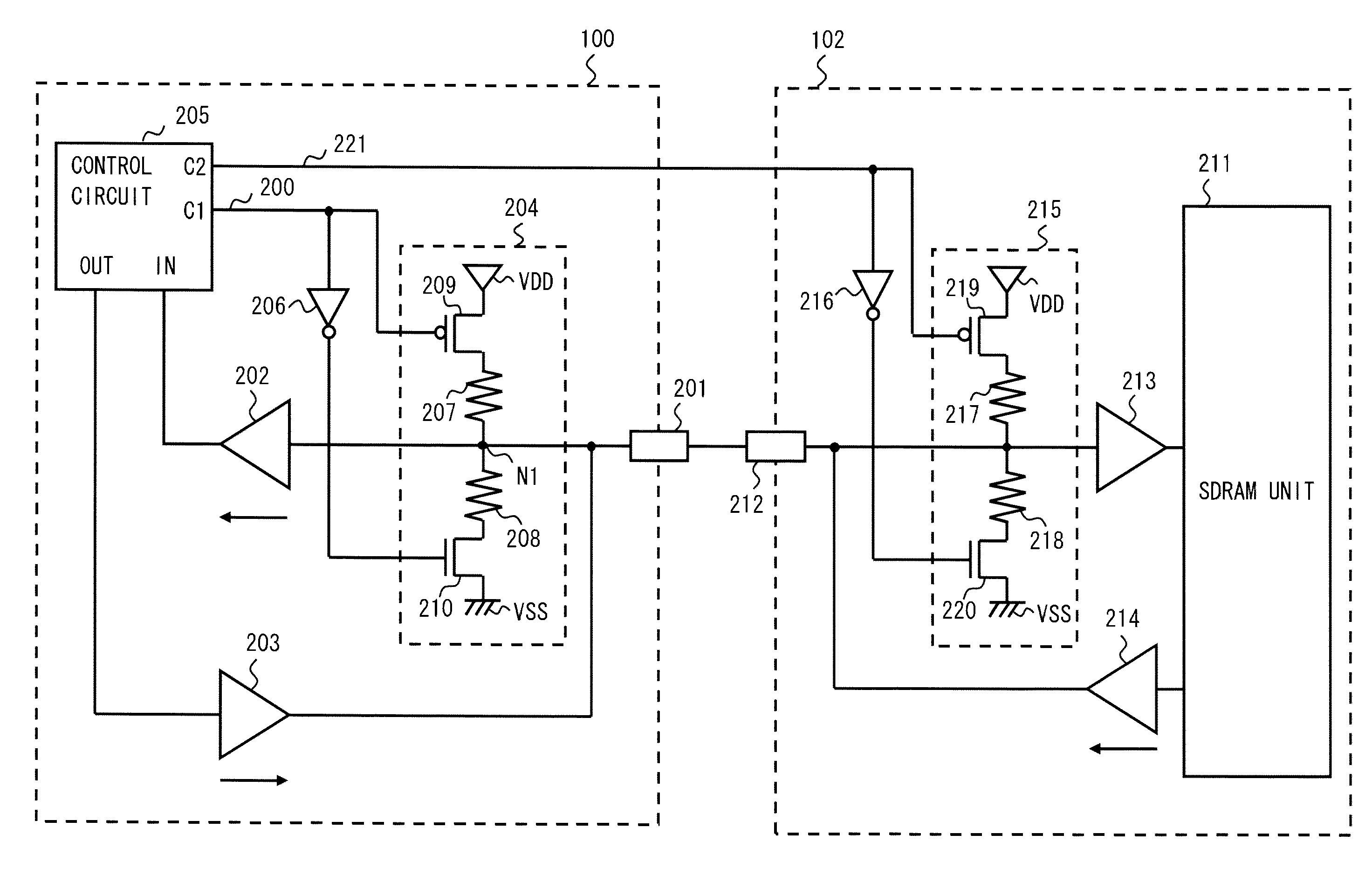
[0046]In the first exemplary embodiment, the case has been explained in which the SoC circuit 100 includes the termination circuit 204. Meanwhile, in this exemplary embodiment, a case is explained in which an SDRAM circuit also includes a termination circuit.

[0047]Referring to FIG. 4, an SDRAM circuit 102 which corresponds to the SDRAM circuit 101 shown in FIG. 2 further includes a termination circuit (second termination circuit) 215. FIG. 4 shows the 1-bit bidirectional signal line, which is one of the strobe signal lines DQS[3:0] and DQSB[3:0] and the data signal line DQ[31:0], and the corresponding peripheral circuits.

[0048]The circuit shown in FIG. 4 includes the SoC circuit 100 and the SDRAM circuit 102. The SDRAM circuit 102 includes an SDRAM unit 211, an external terminal 212, a buffer 213, a buffer 214, a termination circuit 215, and an inverter 216. The termination circuit 215 includes a resistor (second resistor) 217, a resistor 218, a switch (second switch) 219, and a swi...


PUM


Abstract

Provided is a semiconductor integrated circuit according to an exemplary aspect of the present invention including first and second transmitter-receivers that execute transmission and reception of data through a signal line. The first transmitter-receiver includes a first termination circuit that includes a first resistor and a first switch, the first resistor being provided between a first power supply terminal and the signal line, the first switch controlling a current flowing through the first resistor to be turned on and off, and a control circuit that outputs a first control signal to the first termination circuit so that the first switch is turned on when the first transmitter-receiver receives data, the first switch is turned off when the first transmitter-receiver transmits the data, and the first switch is continuously on during a first predetermined period after receiving the data when the first transmitter-receiver further receives another data after receiving the data.

Description

INCORPORATION BY REFERENCE[0001]This application is based upon and claims the benefit of priority from Japanese patent application No. 2009-206881, filed on Sep. 8, 2009, the disclosure of which is incorporated herein in its entirety by reference.BACKGROUND[0002]1. Field of the Invention[0003]The present invention relates to a semiconductor integrated circuit, and more particularly, to a semiconductor integrated circuit suitable for power-supply noise reduction.[0004]2. Description of Related Art[0005]In a semiconductor integrated circuit, there has been a problem that data transmission between transmitter-receivers is not accurately executed when power-supply noise occurs on signal lines used for the data transmission between the transmitter-receivers. To reduce the power-supply noise, reducing the impedance of the signal lines has been required.[0006]Therefore, a countermeasure, for example, ODT (On Die Termination) technique has been provided to reduce the power-supply noise on s...

Claims


Application Information

Patent Timeline
IPC IPC(8): H04B1/10H03K17/00
CPCH03K19/0005G11C11/419G11C7/02H03K19/017545G11C7/22G11C11/4074
Inventor KOMYO, MASAYASUIIZUKA, YOICHI
Owner RENESAS ELECTRONICS CORP
Why Eureka
Try Eureka