

Package substrate and semiconductor apparatus
- Summary
- Abstract
- Description
- Claims
- Application Information
AI Technical Summary
Benefits of technology
Problems solved by technology
Method used
Image

Examples
Embodiment Construction
[0050]The invention will be now described herein with reference to illustrative embodiments. Those skilled in the art will recognize that many alternative embodiments can be accomplished using the teachings of the present invention and that the invention is not limited to the embodiments illustrated for explanatory purposed.
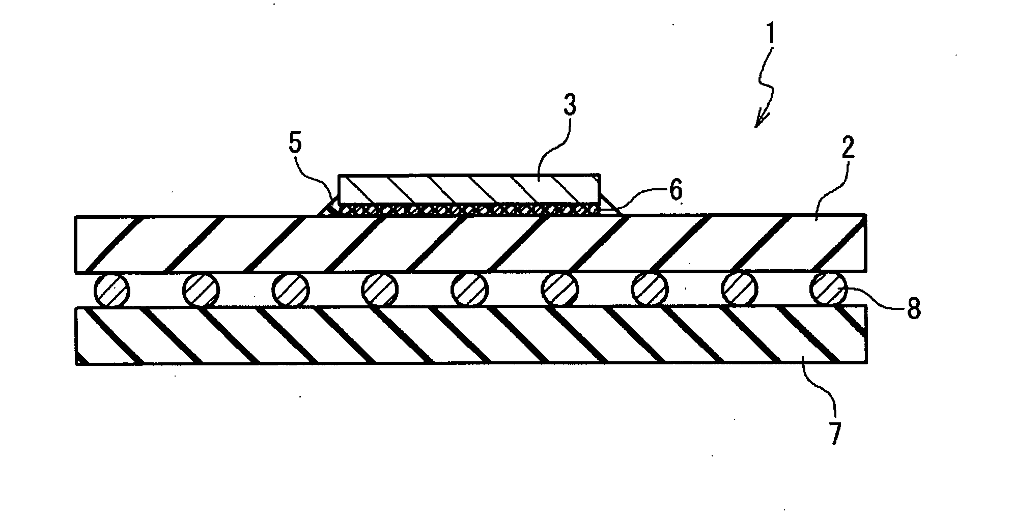
[0051]Embodiments of a semiconductor apparatus according to an embodiment of the present invention will be described below with reference to the attached drawings. As shown in FIG. 5, the semiconductor apparatus 1 includes a package substrate 2, a semiconductor chip 3, resin 5 and a plurality of bumps 6.
[0052]The package substrate 2 is formed into a plate and includes a plurality of electrodes on a surface of the side of the semiconductor chip 3. The semiconductor chip 3 includes a plurality of circuit elements and a plurality of bonding pads. The semiconductor chip 3 generates output electric signals based on input electric signals supplied through some of the p...
PUM
 Abstract
Description
Claims
Application Information