Push compensation in an oscillator

a push compensation and oscillator technology, applied in the direction of oscillation generators, angle modulation details, modulation, etc., can solve the problems of direct frequency change, power supply voltage drop, and even more difficult to meet specifications, so as to reduce power supply noise, reduce oscillator circuit output variation, and reduce supply noise

Inactive Publication Date: 2006-09-21
SILICON LAB INC
View PDF8 Cites 2 Cited by
  • Summary
  • Abstract
  • Description
  • Claims
  • Application Information

AI Technical Summary

Benefits of technology

[0009] It would be desirable to attenuate supply noise across the frequency band without a voltage drop. A design with zero or low Kp provides such attenuation and allows use of a regulator having less stringent requirements in terms of reducing power supply noise.
[0010] Accordingly, according to an embodiment of the invention, a method is provided for compensating for the effects of supply voltage noise on oscillator output. The method includes reducing variation in output of an oscillator circuit caused by variation in a supply voltage for the oscillator circuit, by offsetting a change in a value of a first capacitance in a first direction in response to the variation in the supply voltage with a diode structure having a capacitance that changes in a second direction, opposite the first direction, in response to the variation in the supply voltage.
[0011] In another embodiment the invention provides an oscillator circuit that includes a first capacitance that increases with an increase in a supply voltage coupled to the oscillator circuit. A diode structure, having a second capacitance that decreases with the increase in the supply voltage, offsets the increase in the first capacitance and thereby substantially reduces sensitivity of the oscillator circuit to supply variations.

Problems solved by technology

In such cases supply noise directly translates into frequency change.
Some specifications are even more difficult to meet.
However, an RC filter would tend to drop the power supply voltage, which is undesirable particularly at the low voltage power supplies typical today.
Otherwise, whatever noise is on the regulator output is provided as part of the VCO supply voltage and will translate into phase noise if the VCO is susceptible to pushing.

Method used


Image

  • Push compensation in an oscillator
  • Push compensation in an oscillator
  • Push compensation in an oscillator

Examples


Embodiment Construction

)

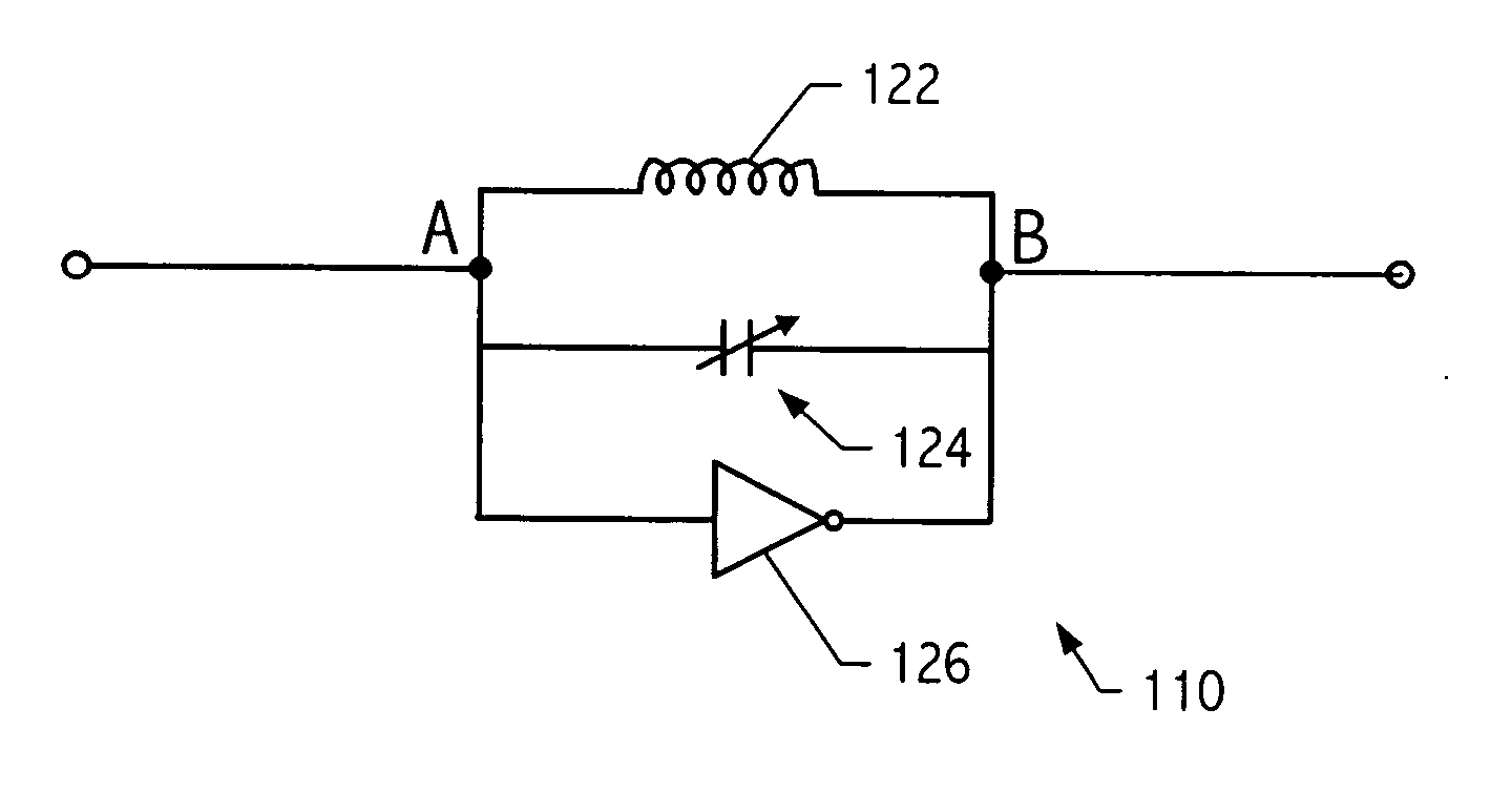
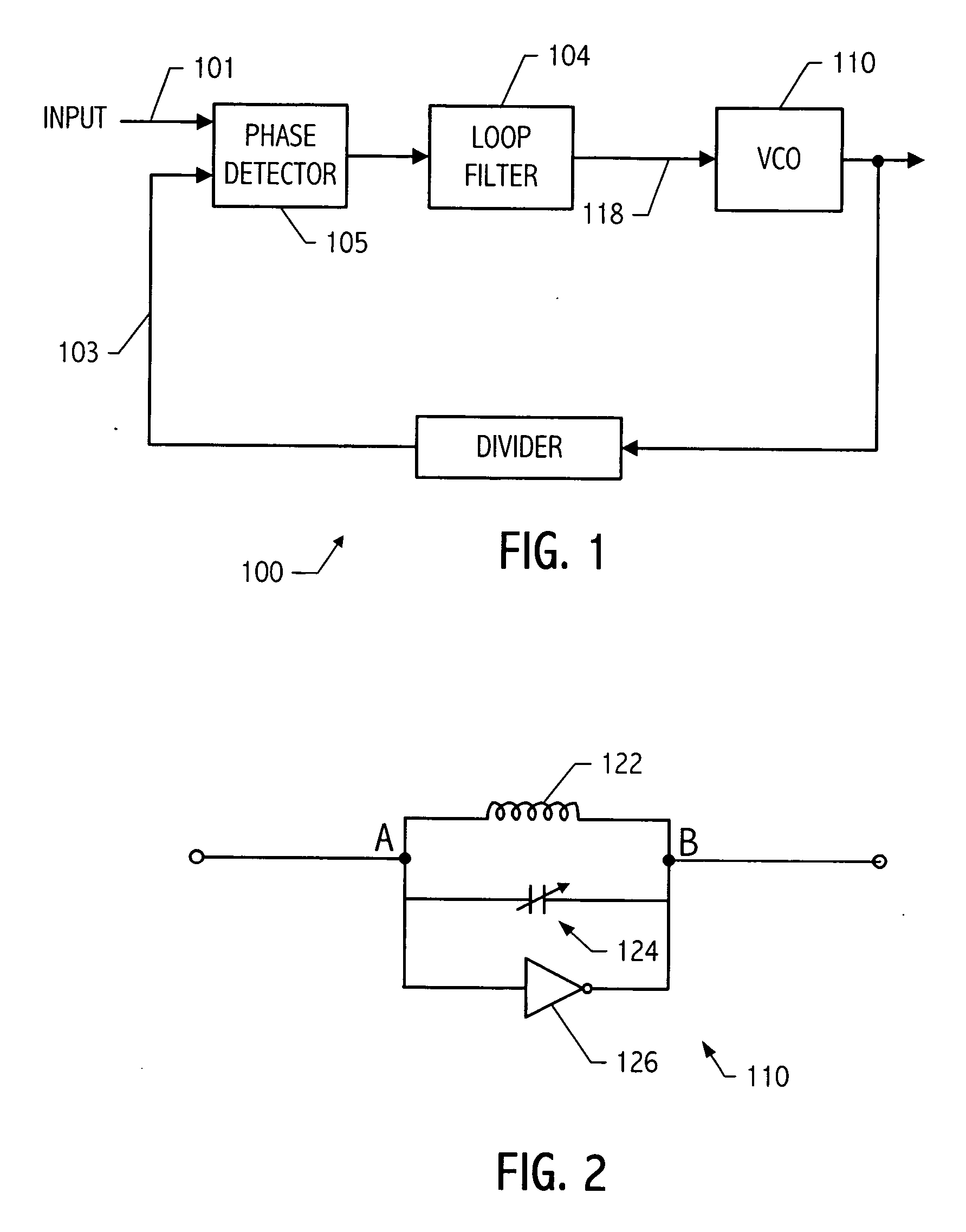
[0025] Referring to FIG. 2, an exemplary VCO circuit is shown. The exemplary VCO circuit is an LC tank circuit and includes an inductor 122, a variable capacitance circuit 124, and a gain or amplifier circuit 126. The output of the VCO can be varied by varying the capacitance circuit 124 in accordance with the control voltage supplied on node 118 (FIG. 1). The oscillating frequency of the VCO is proportional to √{square root over (1 / LC)}.

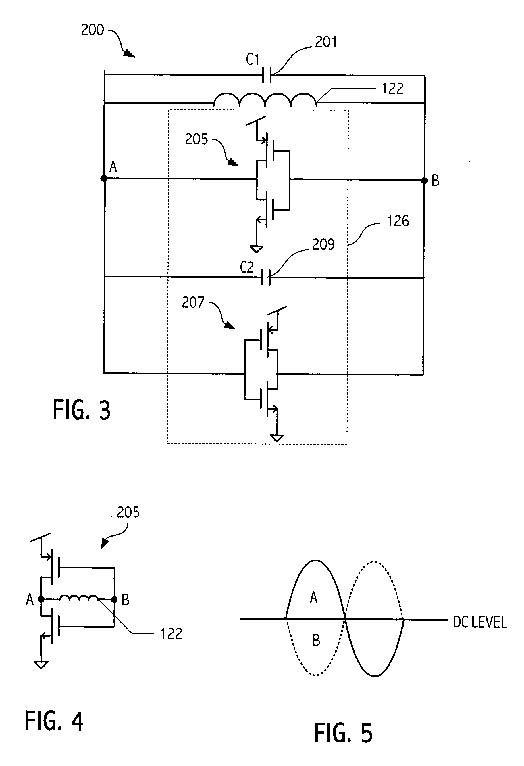
[0026] Referring to FIG. 3, the VCO is shown in more detail. The amplifier circuit 126 includes the inverters 205 and 207. Capacitance is also associated with the amplifier circuit and is represented as capacitance 209 (C2), which is the effective capacitance of the amplifier 126. The capacitance 201 (C1) represents the capacitance of the VCO that is varied to control the VCO output and is relatively constant with respect to supply voltage. The total capacitance of the tank circuit C=C1+C2, where C1 represents the capacitance associated with the v...


PUM


Abstract

The effect of supply voltage variations on an oscillator circuit output are compensated for to reduce supply pushing. The change in a value of a first capacitance in a first direction in response to the variation in the supply voltage is canceled using one or more diodes having a capacitance that changes in a second direction, opposite the first direction, in response to the variation in the supply voltage.

Description

BACKGROUND [0001] 1. Field of the Invention [0002] This application relates to oscillator circuits and more particularly to compensating for the effect of variations in the supply voltage on oscillator output. [0003] 2. Description of the Related Art [0004] Voltage controlled oscillators are commonly found in such applications as phase-locked loop circuits. FIG. 1 illustrates a high level block diagram of a phase-locked loop 100. In the phase-locked loop 100 an input signal 101 and a feedback signal 103 are coupled to a phase / frequency detector 105 that determines the phase / frequency difference between the input signal 101 and the feedback signal 103. That difference is supplied to a loop filter 104, which supplies a control voltage on node 118 to vary the output of the voltage controlled oscillator (VCO) 110 in accordance with the control voltage. The voltage controlled oscillator (VCO) may be implemented using an LC tank circuit in which the oscillating frequency of the VCO is pro...

Claims


Application Information

Patent Timeline
Patent Type & Authority Applications(United States)
IPC IPC(8): H03B5/12
CPCH03B5/04H03K3/011H03K3/354
Inventor ZHANG, LIGANG
Owner SILICON LAB INC
Why Eureka
Try Eureka