Organic electroluminescent device

a technology of electroluminescent devices and organic materials, applied in semiconductor devices, diodes, electrical apparatuses, etc., can solve the problems of relatively reduced light efficiency and achieve the effect of improving light efficiency and brightness, and improving lifetim

Active Publication Date: 2011-03-31
LG DISPLAY CO LTD
View PDF7 Cites 59 Cited by
  • Summary
  • Abstract
  • Description
  • Claims
  • Application Information

AI Technical Summary

Benefits of technology

[0018]An advantage of the present invention is to provide an organic electroluminescent device that can improve lifetime, light efficiency and brightness.
[0019]Additional features and advantages of the present invention will be set forth in the description which follows, and in part will be apparent from the description, or may be learned by practice of the invention. These and other advantages of the invention will be realized and attained by the structure particularly pointed out in the written description and claims hereof as well as the appended drawings.
[0020]To achieve these and other advantages and in accordance with the purpose of the present invention, as embodied and broadly described herein, an electroluminescent device includes: first to third pixel regions; a first electrode in each of the first to third pixel regions, wherein the first electrode of the third pixel region has a first thickness, the first electrode of the first pixel region has a second thickness less than the first thickness, and the first electrode of the second pixel region has a third thickness less than the second thickness; a second electrode in each of the first to third pixel regions; at least two electroluminescent units in each of the first and third pixel regions and disposed between the first electrode and second electrode, wherein one of the at least two electroluminescent units includes a blue light emitting layer and the other of the at least two electroluminescent units include a red / green light emitting layer; and a charge generation layer disposed between the at least two electroluminescent units.
[0021]It is to be understood that both the foregoing general description and the following detailed description are exemplary and explanatory and are intended to provide further explanation of the invention as claimed.

Problems solved by technology

However, the related art OELD does not have the optimized configuration, light efficiency is relatively reduced.

Method used


Image

  • Organic electroluminescent device
  • Organic electroluminescent device
  • Organic electroluminescent device

Examples


Embodiment Construction

[0028]Reference will now be made in detail to illustrated embodiments of the present invention, which are illustrated in the accompanying drawings.

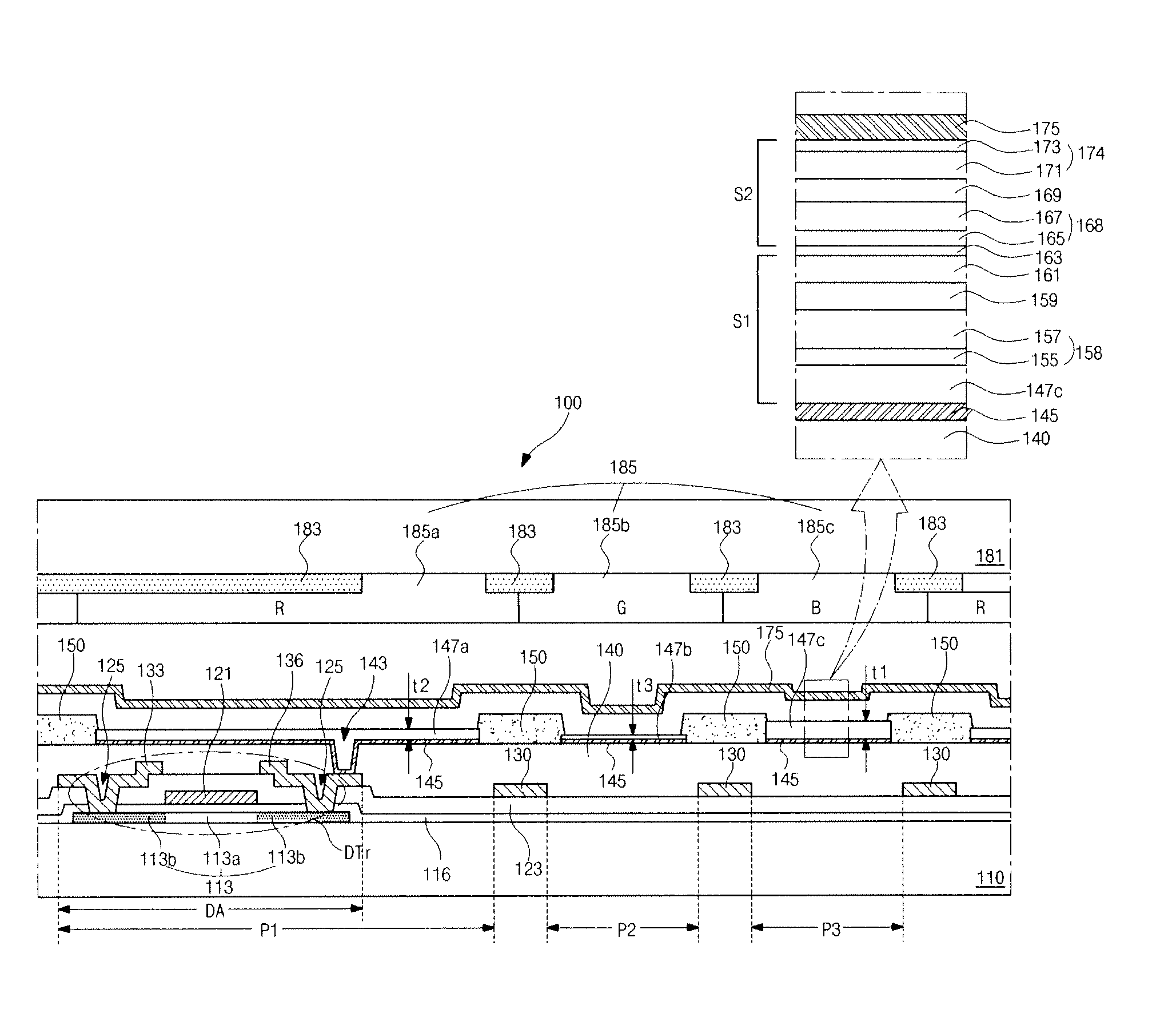
[0029]FIG. 3 is a cross-sectional view illustrating three pixel regions of an OELD according to an embodiment of the present invention. For brevity of explanation, a driving thin film transistor DTr is shown in one pixel region P1 among the three pixel regions P1 to P3. Further, a region, where the driving thin film transistor DTr is formed in each pixel region, is referred to as a driving region DTr, and a region, where the switching thin film transistor (not shown) is formed in each pixel region, is referred to as a switching region (not shown).

[0030]Referring to FIG. 3, the OELD 100 includes first and second substrates 110 and 181 facing each other. The switching thin film transistor, the driving thin film transistor DTr and an organic light emitting diode are formed in each pixel region on the first substrate 101. A color filter layer...


PUM


Abstract

An electroluminescent device includes: first to third pixel regions; a first electrode in each of the first to third pixel regions, wherein the first electrode of the third pixel region has a first thickness, the first electrode of the first pixel region has a second thickness less than the first thickness, and the first electrode of the second pixel region has a third thickness less than the second thickness; a second electrode in each of the first to third pixel regions; at least two electroluminescent units in each of the first and third pixel regions and disposed between the first electrode and second electrode, wherein one of the at least two electroluminescent units includes a blue light emitting layer and the other of the at least two electroluminescent units include a red/green light emitting layer; and a charge generation layer disposed between the at least two electroluminescent units.

Description

[0001]The present invention claims the benefit of Korean Patent Application No. 10-2009-0091363, filed in Korea on Sep. 25, 2009, which is hereby incorporated by reference for all purposes as if fully set forth herein.BACKGROUND OF THE INVENTION[0002]1. Field of the Invention[0003]The present invention relates to an organic electroluminescent device.[0004]2. Discussion of the Related Art[0005]Until recently, display devices have typically used cathode-ray tubes (CRTs). Presently, many efforts and studies are being made to develop various types of flat panel displays, such as liquid crystal displays (LCDs), plasma display panels (PDPs), field emission displays, and electro-luminescence displays (ELDs), as a substitute for CRTs. Of these flat panel displays, organic electroluminescent displays (OELDs) are self-luminescent display devices. The OELD operate at low voltages and have a thin profile. Further, the OELD have fast response time, high brightness, and wide viewing angles.[0006]...

Claims


Application Information

Patent Timeline
Patent Type & Authority Applications(United States)
IPC IPC(8): H01L51/52
CPCH01L27/3211H01L27/322H01L51/5278H01L51/5265H01L27/3246H10K59/35H10K59/38H10K59/122H10K50/852H10K50/19H10K2102/351
Inventor KIM, CHANG-OHKIM, HWA-KYUNGPIEH, SUNG-HOON
Owner LG DISPLAY CO LTD
Why Eureka
Try Eureka