Anti-static housing and related display device assembly

a display device and anti-static technology, applied in the direction of electric apparatus casings/cabinets/drawers, furniture parts, instruments, etc., can solve the problems of inefficiency of assembly, prone to failure of strict esd tests, and display devices b>12/b> of the conventional display device module b>1/b> being prone to adverse effects of static electricity, etc., to achieve enhanced anti-static characteristics, reduce assembly cost, and facilitate assembly

Active Publication Date: 2011-03-31
WISTRON CORP
View PDF3 Cites 6 Cited by
  • Summary
  • Abstract
  • Description
  • Claims
  • Application Information

AI Technical Summary

Benefits of technology

[0010]Therefore, one object of the present invention is to provide an anti-static housing that is easy to assemble on a display device so as to reduce assembly costs.
[0018]The merit of the present invention resides in that when the first and second housing bodies of the anti-static housing are coupled together, the first and second rail-and-groove engaging structures are disposed so as to impede passage of static electricity through gaps between the first and second housing bodies, and the anti-static dielectric layers disposed between adjacent pairs of the first and second lateral walls further impede such passage of static electricity. The anti-static housing of the present invention thus has enhanced anti-static characteristics. In addition, use of the first and second rail-and-groove engaging structures facilitates assembly of the anti-static housing and reduces assembly cost.

Problems solved by technology

The ESD test often reveals that the display device 12 of the conventional display device module 1 is prone to adverse effects from static electricity.
The conventional display device module 1 is thus prone to fail strict ESD tests required in some countries.
Moreover, since the first and second housing bodies 111,112 are fastened together with the use of screws, assembly is inefficient and results in higher assembly costs.

Method used


Image

  • Anti-static housing and related display device assembly
  • Anti-static housing and related display device assembly
  • Anti-static housing and related display device assembly

Examples


Embodiment Construction

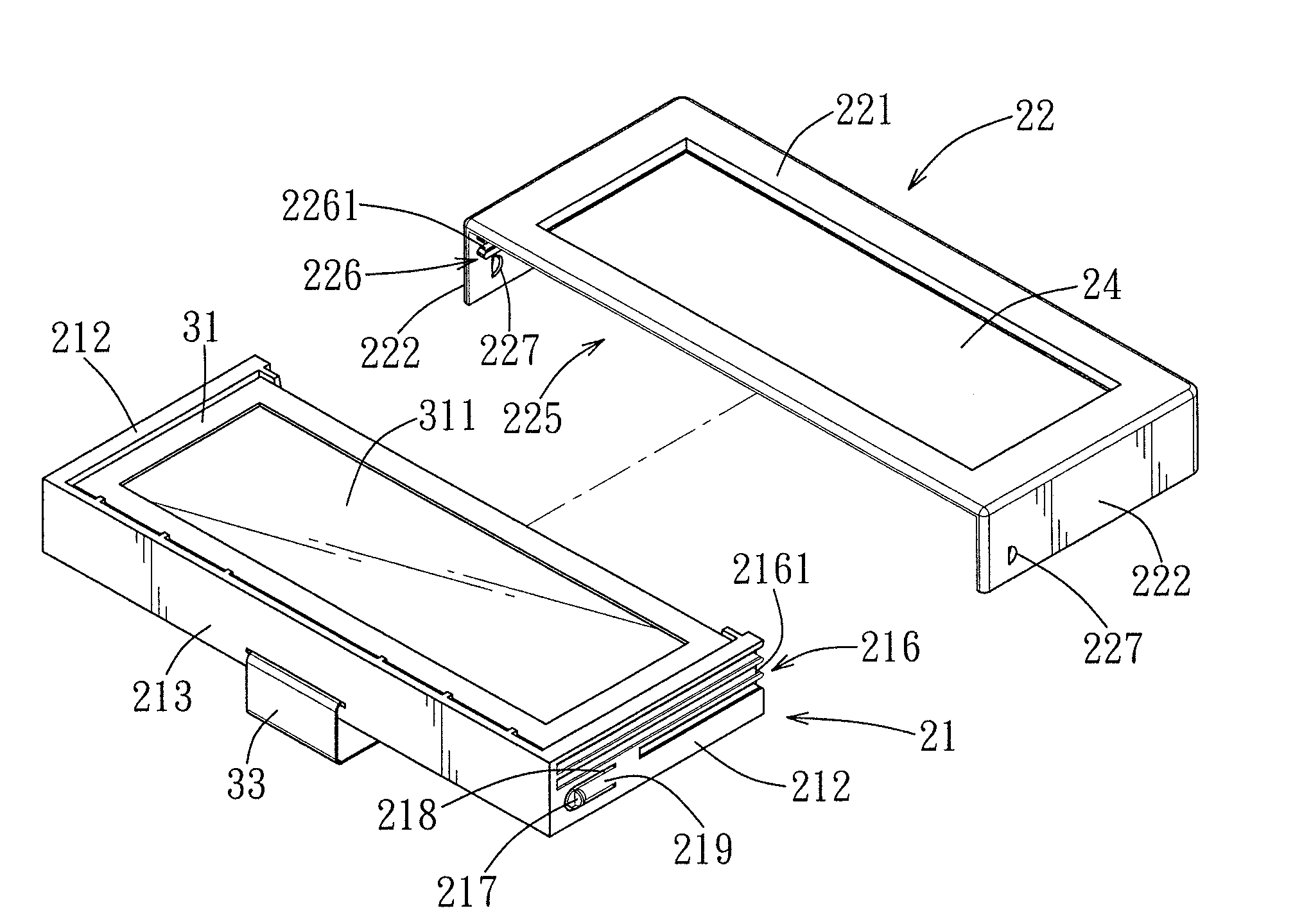
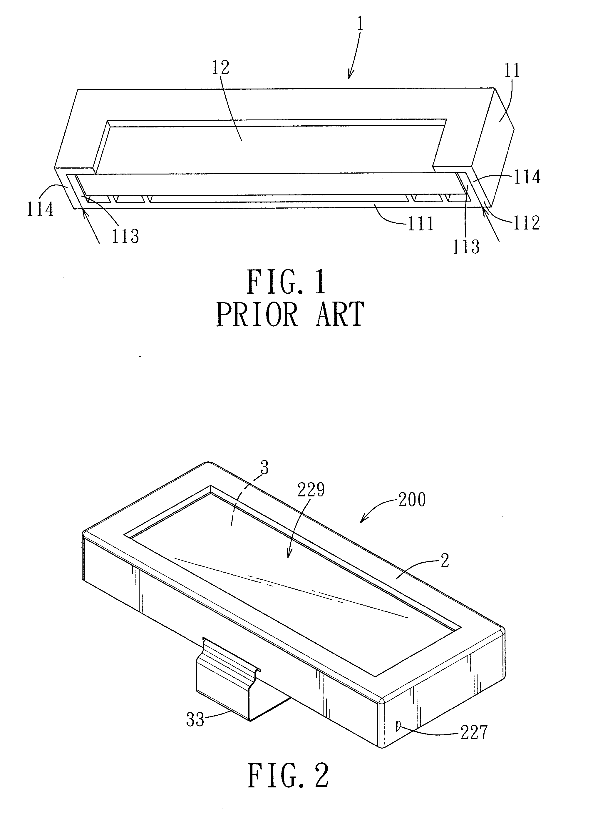
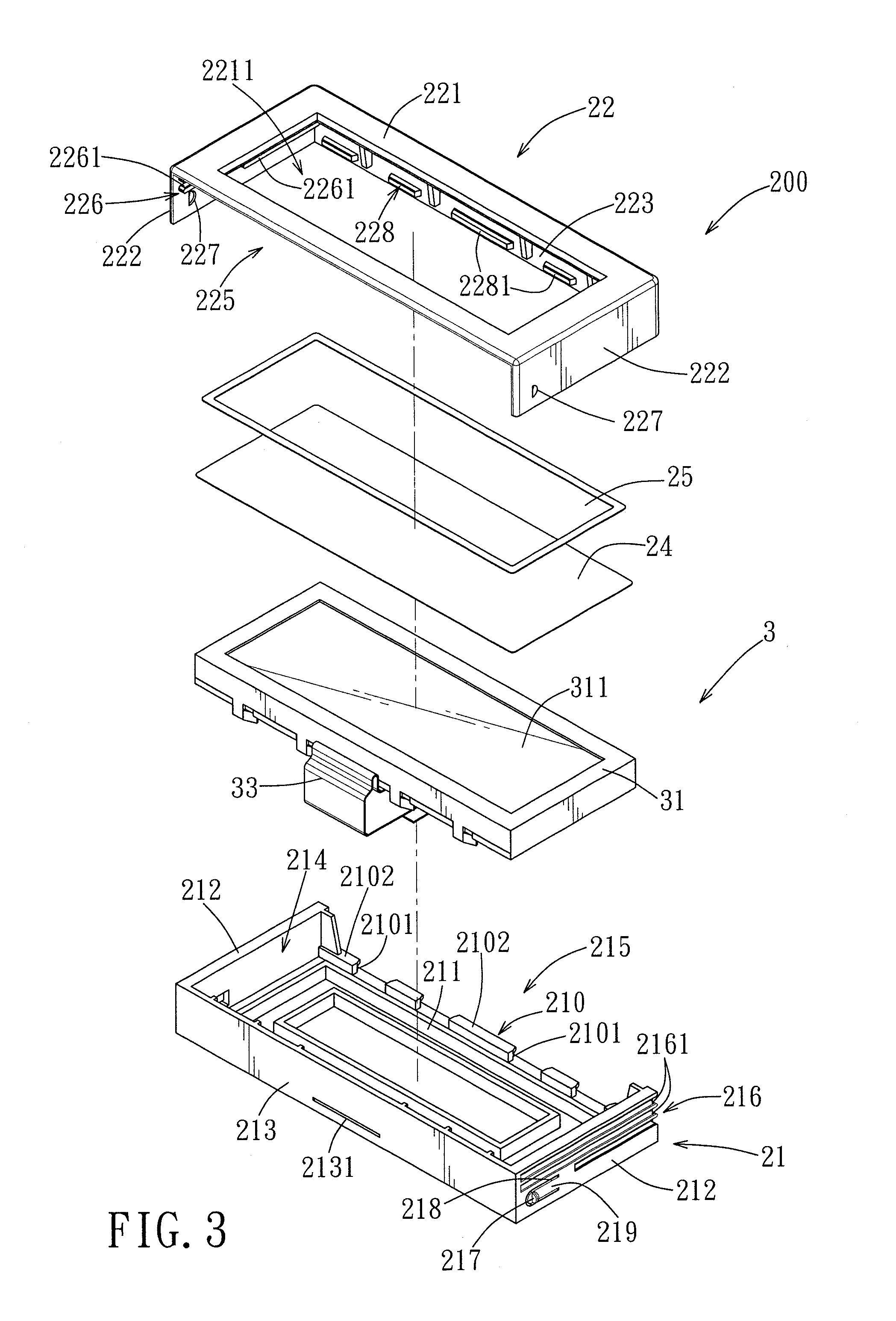
[0028]FIG. 2 illustrates the preferred embodiment of a display device assembly 200 according to the present invention. The display device assembly 200 comprises a anti-static housing 2 and a displaying module 3. In this embodiment, the display device assembly 200 is adapted to be coupled to a telephone so as to provide the telephone with video display functionality. However, application of the display device assembly 200 is not limited to what is disclosed herein. The display device assembly 200 can be adapted to provide display functionality to another type of electronic device.

[0029]Referring to FIGS. 2, 3 and 7, the anti-static housing 2 has a first housing body 21, a second housing body 22 and a plurality of anti-static dielectric layers 23.

[0030]The first housing body 21 includes a bottom wall 211, a pair of first lateral walls 212 spaced apart from each other and extending upward from left and right edges of the bottom wall 211, and a first connecting wall 213 extending upward...


PUM


Abstract

A display device assembly includes an anti-static housing and a displaying module contained therein. The anti-static housing has a first housing body, a second housing body and a plurality of anti-static dielectric layers. The first housing body and the second housing body respectively have a first rail-and-groove engaging structure and a second rail-and-groove engaging structure, and can be moved relative to each other such that the first rail-and-groove engaging structure engages the second rail-and-groove engaging structure. Due to dispositions of the first and second rail-and-groove engaging structures and the anti-static dielectric layers when the first and second housing bodies are coupled together, the anti-static housing has comparatively superior anti-static characteristics, and a manner of engagement between the first and second rail-and-groove engaging structures facilitates assembly of the anti-static housing and thus reduces assembly costs.

Description

CROSS-REFERENCE TO RELATED APPLICATION[0001]This application claims priority of Taiwanese application no. 098217759, filed on Sep. 25, 2009.BACKGROUND OF THE INVENTION[0002]1. Field of the Invention[0003]The invention relates to a display device assembly, more particularly to an anti-static housing and a displaying module assembled in a display device.[0004]2. Description of the Related Art[0005]Prior to delivery, common electronic devices such as mobile phones, display devices, and computers are typically tested to determine their degree of susceptibility to electrostatic discharge (ESD). The ESD test is conducted in order to ensure that internal electronic components of the electronic devices are not susceptible to damage or signal interference from electrostatic discharge generated by use of the electronic devices in a dry environment or in an environment otherwise prone to generating electrostatic discharge.[0006]Referring to FIG. 1, a conventional display device module 1 used i...

Claims


Application Information

Patent Timeline
Patent Type & Authority Applications(United States)
IPC IPC(8): H05K5/00A47B81/00
CPCG02F1/133308G02F2202/22H04M1/0266G06F1/1607G06F1/1637G06F1/1601
Inventor KUO, YU-LING
Owner WISTRON CORP
Why Eureka
Try Eureka