Antenna module and method for manufacturing the same

a technology of antenna modules and antenna modules, which is applied in the field of antenna modules, can solve the problems of complex assembling process and increase in the manufacturing cost of terahertz antenna modules, and achieve the effects of reducing the manufacturing cost of antenna modules 500, reducing the manufacturing cost, and facilitating assembly

Inactive Publication Date: 2014-08-14
NITTO DENKO CORP
View PDF5 Cites 225 Cited by
  • Summary
  • Abstract
  • Description
  • Claims
  • Application Information

AI Technical Summary

Benefits of technology

[0014]Here, the transmission loss α [dB / m] of the electromagnetic wave is expressed in the following formula by a conductor loss α1 and a dielectric loss α2.
[0137]In the method for manufacturing the antenna module 500 according to the present embodiment, the support layer 210 of the support body 200 is formed on the back surface of the dielectric film 10, and the dielectric lens 300 is provided on the support layer 210 with the insulating layer 220 sandwiched therebeteween. Thereafter, the support layer 210 is bent along the bent portions F1 to F4 such that the electromagnetic wave in the terahertz band that is transmitted or received by the electrodes 20a, 20b permeates through the dielectric lens 300.
[0138]In this case, it is possible to arrange the dielectric lens 300 at a position at which the light axis of the dielectric lens 300 passes through the tapered slot S of the antenna portion 100 by bending the support layer 210 without using a plurality of attachment members. Therefore, a manufacturing cost for the antenna module 500 is reduced, and the antenna module 500 can be easily assembled.
[0139]Further, in the antenna module 500 according to the present embodiment, the electromagnetic wave in the terahertz band is transmitted or received by the electrodes 20a, 20b formed on the main surface of the dielectric film 10. Further, the semiconductor device 30 mounted on the main surface of the dielectric film 10 performs detection and rectification, or oscillation. The electromagnetic wave transmitted or received by the electrodes 20a, 20b are converged or paralleled by permeating through the dielectric lens 300.
[0140]Further, because the dielectric film 10 is formed of resin, an effective relative permittivity of the surroundings of the electrodes 20a, 20b is low. Thus, the electromagnetic wave radiated from the electrodes 20a, 20b or received by the electrodes 20a, 20b is less likely attracted to the dielectric film 10. Therefore, the electromagnetic wave can be efficiently radiated, and better directivity of the antenna module 500 is obtained.
[0142]Letting ∈ref be an effective relative permittivity, f be a frequency, R(f) be conductor surface resistance and tan δ be a dielectric tangent, the conductor loss α1 and the dielectric loss α2 are expressed as below.

Problems solved by technology

Therefore, a manufacturing cost of the terahertz antenna module increases, and an assembling process of the terahertz antenna module is complicated.

Method used


Image

  • Antenna module and method for manufacturing the same
  • Antenna module and method for manufacturing the same
  • Antenna module and method for manufacturing the same

Examples


first embodiment

[1] First Embodiment

(1) Configuration of Antenna Module

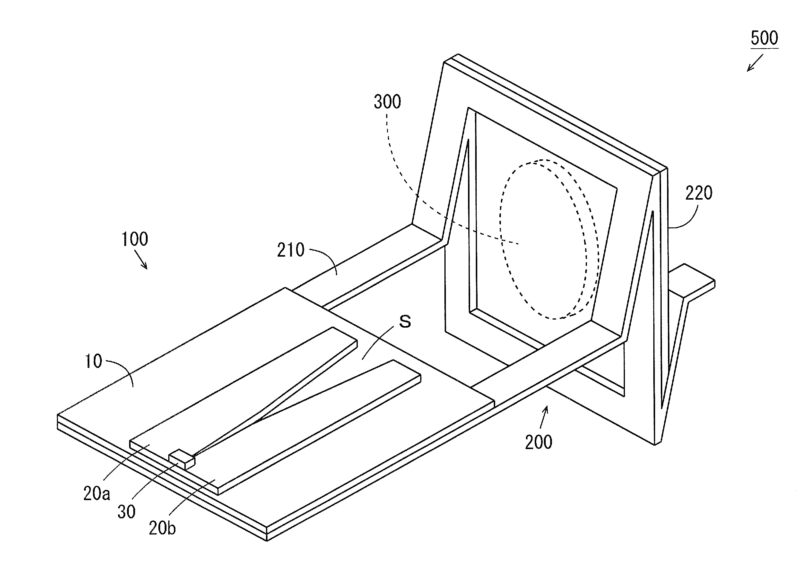
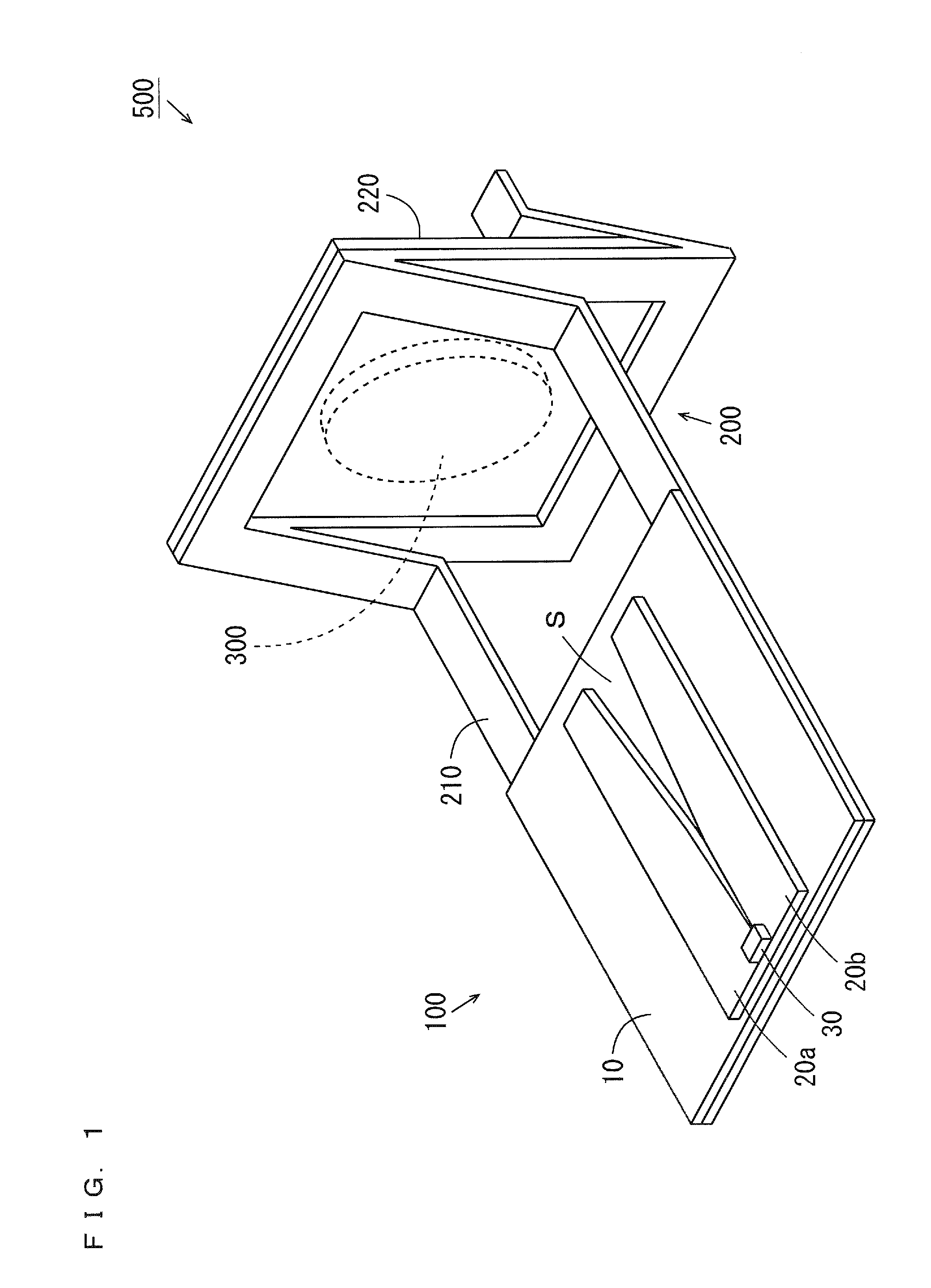
[0088]FIG. 1 is an external perspective view of the antenna module according to the first embodiment. FIG. 2 is a schematic side view of the antenna module of FIG. 1. As shown in FIGS. 1 and 2, the antenna module 500 includes an antenna portion 100, a support body 200 and a dielectric lens 300. Details of the antenna portion 100, the support body 200 and the dielectric lens 300 will be described below.

[0089]FIG. 3 is a schematic plan view of the antenna portion 100 of FIG. 1. FIG. 4 is a cross sectional view taken along the line A-A of the antenna portion 100 of FIG. 3. As shown in FIGS. 3 and 4, the antenna portion 100 is constituted by a dielectric film 10, a pair of electrodes 20a, 20b and a semiconductor device 30. The dielectric film 10 is formed of resin that is made of polymer. One surface of the two surfaces of the dielectric film 10 opposite to each other is referred to as a main surface, and the other surface is referr...

second embodiment

[2] Second Embodiment

(1) Configuration of Antenna Module

[0145]Regarding the antenna module according to the second embodiment, difference from the antenna module 500 according to the first embodiment will be described. FIG. 17 is an external perspective view of the antenna module according to the second embodiment. FIG. 18 is a schematic side view of the antenna module of FIG. 17. As shown in FIGS. 17 and 18, the antenna module 500 includes the antenna portion 100, the support body 200 and the dielectric lens 300. The configuration of the antenna portion 100 in the present embodiment is similar to the configuration of the antenna portion 100 in the first embodiment. Details of the support body 200 and the dielectric lens 300 will be described below.

[0146]The support body 200 according to the present embodiment includes the support layer 210 and a lens holding member 240. The lens holding member 240 is formed of material having a shape-retaining property. In the present embodiment, t...


PUM


Abstract

An electrode is formed on at least one surface of first and second surfaces of a dielectric film formed of resin to be capable of receiving or transmitting an electromagnetic wave in a terahertz band. A semiconductor device operable in the terahertz band is mounted on at least one surface of the first and second surfaces of the dielectric film to be electrically connected to the electrode. A portion of a support layer is formed on the first or second surface of the dielectric film, and a dielectric lens is supported by another portion of the support layer. Another portion of the support layer is bent with respect to the portion such that the electromagnetic wave in the terahertz band transmitted or received by the electrode permeates through the dielectric lens.

Description

BACKGROUND OF THE INVENTION[0001]1. Field of the Invention[0002]The present invention relates to an antenna module that transmits or receives an electromagnetic wave of a frequency in a tera hertz band not less than 0.05 THz and not more than 10 THz, for example.[0003]2. Description of Related Art[0004]Terahertz transmission using an electromagnetic wave in the terahertz band is expected to be applied to various purposes such as short-range super high speed communication and uncompressed delayless super high-definition video transmission.[0005]In JP 2008-244620 A, a terahertz antenna module having a photoconductive antenna device is described. In the photoconductive antenna device, a pair of ohmic electrodes is formed at a GaAs layer on a semi-insulating GaAs substrate. A photoconductive antenna portion is formed by part of the pair of ohmic electrodes. This terahertz antenna module includes a rectangular parallelepiped base made of metal. A buffer member, a hemisphere-shaped lens, ...

Claims


Application Information

Patent Timeline
Patent Type & Authority Applications(United States)
IPC IPC(8): H01L31/0232H01L31/12
CPCH01L31/12H01L31/02325H01Q1/1264H01Q13/085H01Q19/062
Inventor INOUE, MASAMIHODONO, MASAYUKIHONJO, MITSURU
Owner NITTO DENKO CORP
Why Eureka
Try Eureka