Semiconductor package with integrated interference shielding and method of manufacture thereof

a technology of interference shielding and semiconductor devices, applied in the direction of semiconductor devices, semiconductor/solid-state device details, electrical equipment, etc., can solve the problems of lack of design flexibility, high cost, and metal can add significant size to the device footprint of printed circuit boards, and achieve reliable electrical connections and robust manufacturing processes.

Active Publication Date: 2011-04-14
SKYWORKS SOLUTIONS INC
View PDF4 Cites 84 Cited by
  • Summary
  • Abstract
  • Description
  • Claims
  • Application Information

AI Technical Summary

Benefits of technology

[0007]Aspects and embodiments of the present invention are directed to a semiconductor device package, and methods of making the same, that uses wirebond process technologies to integrate an electromagnetic interference shield into the device package. In one embodiment, wirebond processes are used to form wirebond springs that are positioned around the device and coupled to conductive layers above and below the device, thereby forming an electromagnetic interferen...

Problems solved by technology

The traditional method of isolating RF devices from such electromagnetic interference is to cover the RF device with a grounded metal enclosure typically called a “can.” However, this solu...

Method used


Image

  • Semiconductor package with integrated interference shielding and method of manufacture thereof
  • Semiconductor package with integrated interference shielding and method of manufacture thereof
  • Semiconductor package with integrated interference shielding and method of manufacture thereof

Examples


Embodiment Construction

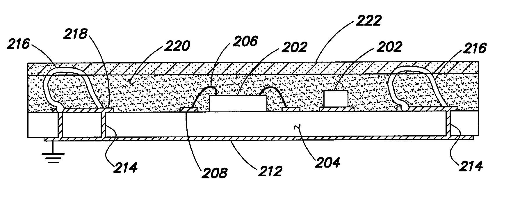
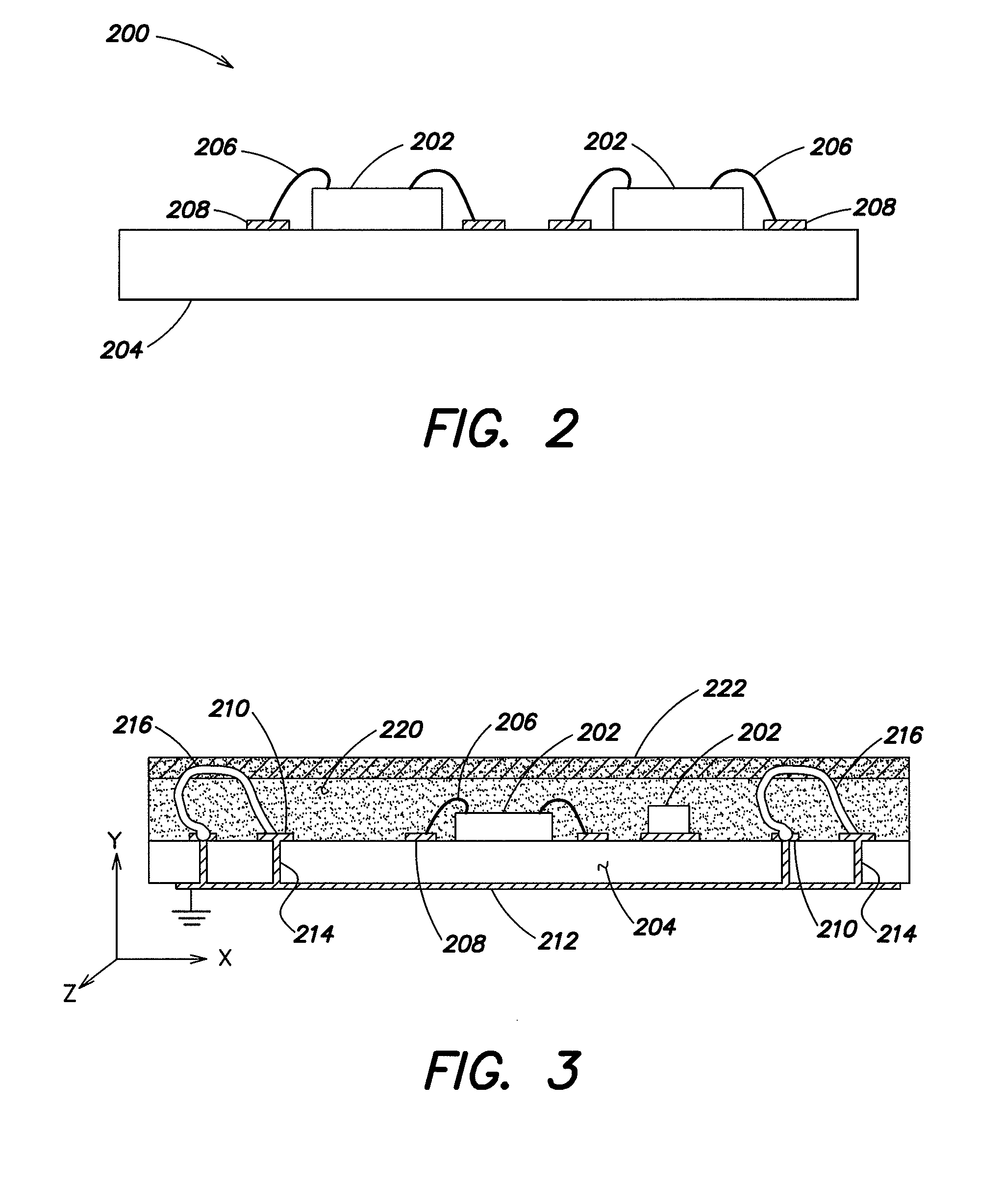
[0027]In many modem applications, including cellular phone handsets, personal digital assistants (PDAs), media players, and other portable device that use radio frequency (RF) components, the size (length, width and thickness) and weight of the finished product can often be critical design parameters. For example, particularly for cellular phone handsets, there is continuing drive toward smaller and lighter devices that offer increased functionality and features. Accordingly, the size and weight of individual components used in these devices can also be important. As discussed above, the conventional approach for providing electromagnetic interference shielding for RF devices involves placing a grounded metal can over the individual RF device to be shielded, which adds size, weight and cost to the design and therefore, may be undesirable in many applications.

[0028]Aspects and embodiments are directed to methods and apparatuses to provide an interference shield that is integrated int...


PUM


Abstract

An integrated electromagnetic interference (EMI) shield for a semiconductor module package. The integrated EMI shield includes a plurality of wirebond springs electrically connected between a ground plane in the substrate of the package and a conductive layer printed on the top of the package mold compound. The wirebond springs have a defined shape that causes a spring effect to provide contact electrical connection between the tops of the wirebond springs and the conductive layer. The wirebond springs can be positioned anywhere in the module package, around all or some of the devices included in the package, to create a complete EMI shield around those devices.

Description

CROSS-REFERENCE TO RELATED APPLICATIONS[0001]This application is a continuation of and claims priority under 35 U.S.C. §§120 and 363 to International Application No. PCT / US2008 / 071832 filed Jul. 31, 2008 and titled “SEMICONDUCTOR PACKAGE WITH INTEGRATED INTERFERENCE SHIELDING AND METHOD OF MANUFACTURE THEREOF,” which is herein incorporated by reference in its entirety.BACKGROUND[0002]1. Field of Invention[0003]The present invention is directed to semiconductor device packages and, more particularly, to electromagnetic and / or radio frequency interference shielding for semiconductor devices.[0004]2. Discussion of Related Art[0005]There exists a general need in radio frequency (RF) communication systems for RF devices to be isolated from electromagnetic (radio frequency) interference (EMI) generated by other RF devices in order to maintain proper device performance. Similarly, the RF devices generally need to be isolated from the electromagnetic interference received from, or transmitt...

Claims


Application Information

Patent Timeline
IPC IPC(8): H01L23/552H01L21/50
CPCH01L21/56H01L2224/4945H01L23/552H01L2224/48227H01L2924/01079H01L2924/3025H01L24/48H01L2224/45144H01L2224/45147H01L23/3121H01L24/33H01L24/49H01L2224/33181H01L2224/48091H01L2224/4909H01L2924/19107H01L21/50H01L2224/16225H01L2924/01047H01L2224/49096H01L2924/00H01L24/45H01L2224/29339H01L2924/181H01L2924/12042H01L2224/85207H01L2924/00014H01L2924/00012
Inventor WELCH, PATRICK L.GUO, YIFAN
Owner SKYWORKS SOLUTIONS INC
Why Eureka
Try Eureka