

Pin-out Designation Method for Package-Board Codesign
a technology of package board and pinout, which is applied in the direction of instruments, semiconductor devices, computing, etc., can solve the problems of reducing signal performance, affecting signal quality, and affecting the design of packaging for accommodating chips, so as to achieve the effect of preserving signal quality
- Summary
- Abstract
- Description
- Claims
- Application Information
AI Technical Summary
Benefits of technology
Problems solved by technology
Method used
Image

Examples
Embodiment Construction
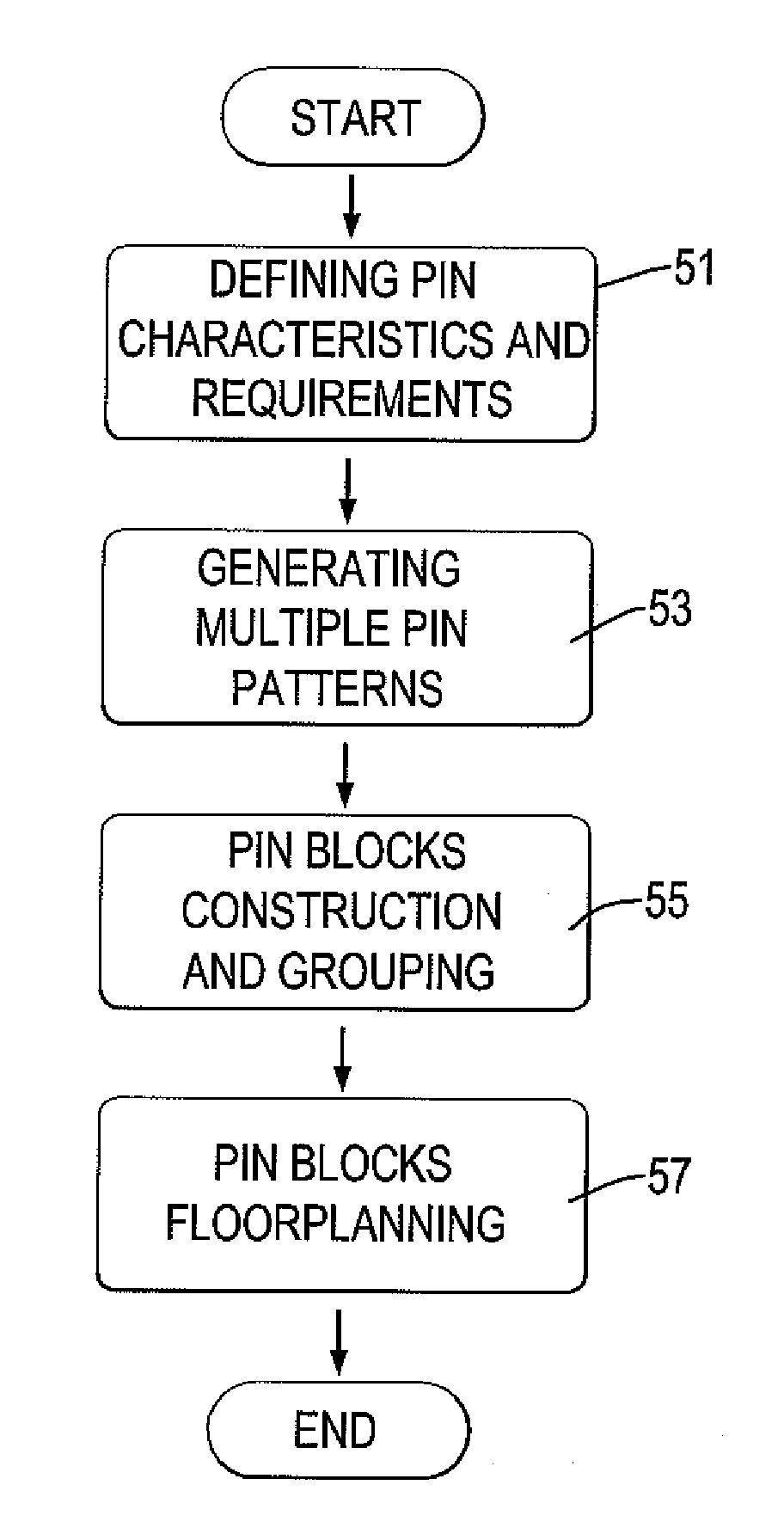
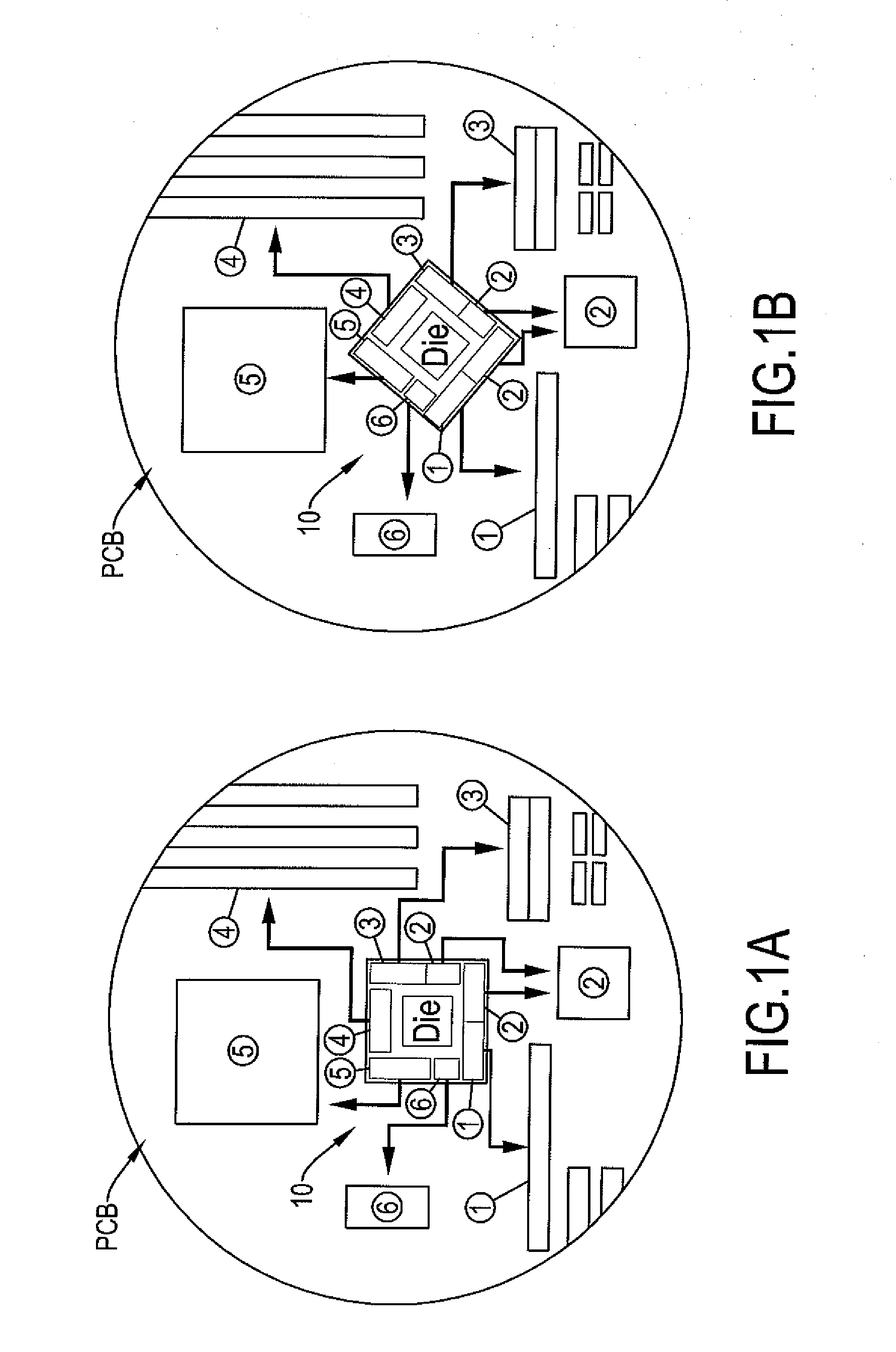
[0022]With reference to FIGS. 1A and 1B, to understand the pin out designation method for package board codesign in accordance with the present invention, considerations and critical constrains in designating pin-out for a chip (10) are stated as follows.
[0023]I. Pin Out Designation by Considering Signal Integrity and Power Delivery in Package-Board Codesign
[0024]When designating pin-out, there are several critical constraints and considerations requiring care. A discussion is provided to introduce a design of pin pattern which can take all the constraints and considerations into account.
[0025]A. Constraints and Considerations
[0026]1) Locations of PCB Components:
[0027]With reference to FIGS. 1A and 1B, which depict two sketches of two different PCB layouts that have different signal nets. Usually, PCB contains several kinds of components and connectors (numbered as 1 to 5) which are applied to specific interfaces. A chip (10) is mounted between those components and connectors and ha...
PUM
 Abstract
Description
Claims
Application Information