Organic/inorganic composite comprising three-dimensional carbon nanotube networks, method for preparing the organic/inorganic composite and electronic device using the organic/inorganic composite
a carbon nanotube and organic/inorganic composite technology, applied in the field of organic/inorganic composite comprising three-dimensional carbon nanotube networks, can solve the problems of poor processing efficiency, marked decrease in the density of the network, and difficulty in directly applying the method to the fabrication of electronic devices, etc., to achieve high electrical conductivity, improve efficiency, and large surface area
- Summary
- Abstract
- Description
- Claims
- Application Information
AI Technical Summary
Benefits of technology
Problems solved by technology
Method used
Image

Examples
example 1
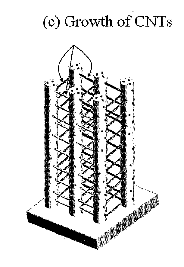
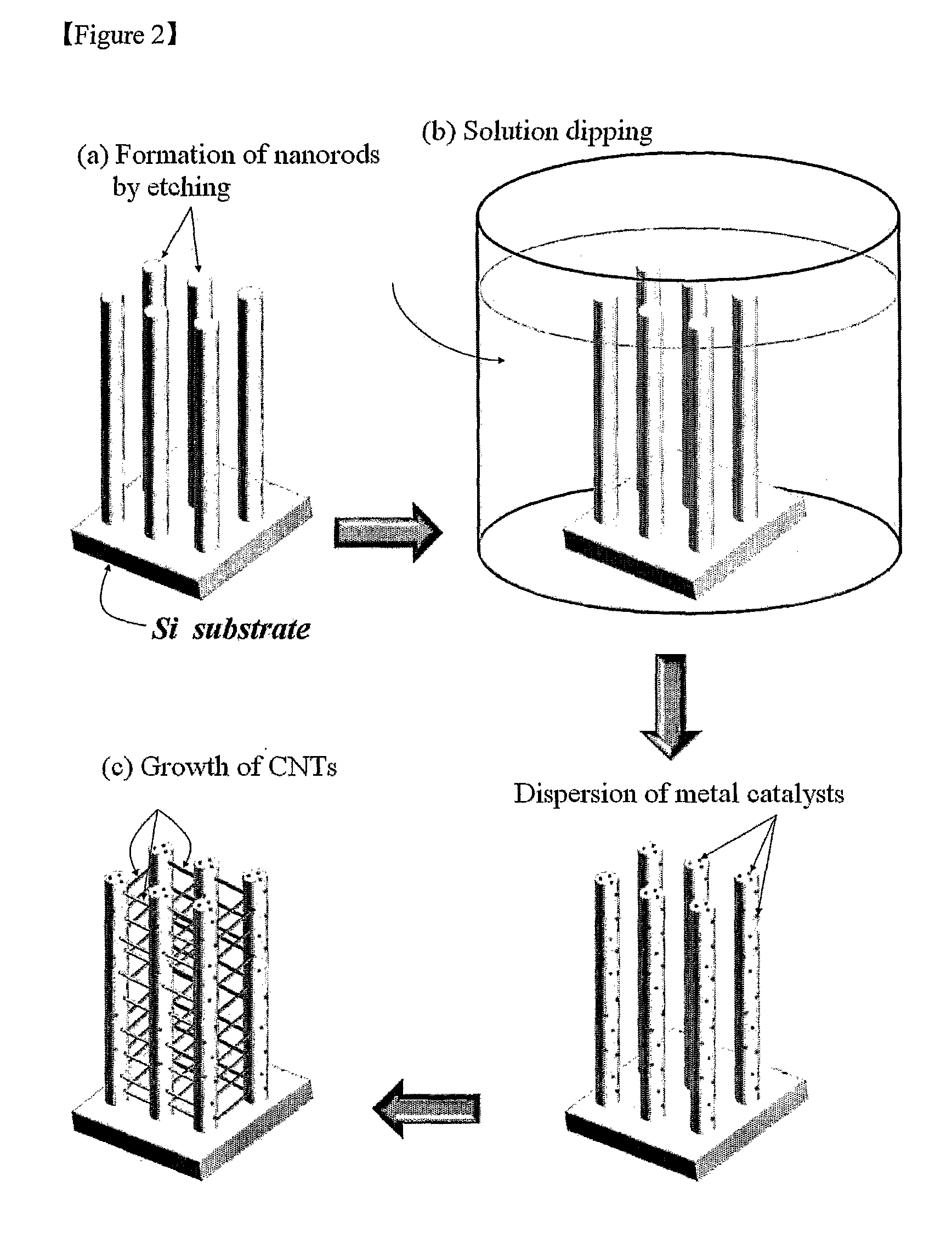
[0063]An n-type Si wafer was etched by common photolithography and the Bosch process to form nanorods having a height of 2 μm and a diameter of about 1 μm. The nanorods were spaced apart from each other at intervals of 1 μm. Then, the etched Si wafer was cleaned with acetone, ethanol and deionized water, treated with piranha solution for 30 min to modify the surface of the Si wafer into Si—OH, and cleaned with deionized water. An ethanolic solution of Fe(NO3)3.9H2O (Junsei, Japan) was mixed with an aqueous solution of molybdenum (ICP / DCP standard solution, 10,000 μg / mL Mo in H2O, Aldrich) to prepare a catalyst solution. The molar concentration ratio of Fe to Mo in the catalyst solution was adjusted to 4:1. The surface-modified Si wafer was dipped in the catalyst solution to uniformly adsorb the catalysts over the entire surfaces of the wafer and the nanorods, cleaned with ethanol, and mounted in a horizontal quartz tube reactor. The Si wafer adsorbed by the catalysts was annealed in...
example 2
[0064]Three-dimensional networks of single-walled carbon nanotubes were formed in the same manner as in Example 1, except that the nanorods had a height of 5 μm and a diameter of about 0.75 μm and were spaced apart from each other at intervals of 1.25 μm.
example 3
[0065]Three-dimensional networks of single-walled carbon nanotubes were formed in the same manner as in Example 1, except that the nanorods had a height of 7 μm and a diameter of about 1.3 μm and were spaced apart from each other at intervals of 1.3 μm.
PUM
| Property | Measurement | Unit |
|---|---|---|
| Height | aaaaa | aaaaa |
| Height | aaaaa | aaaaa |
| Volume | aaaaa | aaaaa |
Abstract
Description
Claims
Application Information
 - R&D Engineer
- R&D Manager
- IP Professional
- Industry Leading Data Capabilities
- Powerful AI technology
- Patent DNA Extraction
Browse by: Latest US Patents, China's latest patents, Technical Efficacy Thesaurus, Application Domain, Technology Topic.
© 2024 PatSnap. All rights reserved.Legal|Privacy policy|Modern Slavery Act Transparency Statement|Sitemap