System and method for correcting systematic parametric variations on integrated circuit chips in order to minimize circuit limited yield loss

a technology of integrated circuit chips and systematic parametric variations, applied in stochastic cad, cad techniques, instruments, etc., can solve the problems of significant device performance variation, will not/do not meet pre-defined performance expectations, and circuit limited yield loss, so as to minimize regional parametric variations and minimize circuit limited yield loss

Inactive Publication Date: 2011-04-28
GLOBALFOUNDRIES INC
View PDF1 Cites 3 Cited by
  • Summary
  • Abstract
  • Description
  • Claims
  • Application Information

AI Technical Summary

Benefits of technology

[0005]In view of the foregoing, disclosed herein are embodiments of a system and an associated method of correcting systematic, design-based, parametric variations on integrated circuit chips in order to minimize circuit limited yield loss without incurring significant cost and time penalties. In the embodiments, processing information is stored. This processing information can indicate a relative impact, on a given device parameter, of changes in a value for a specification associated with a given process step. Additionally, a map of an integrated circuit chip is stored. This map can indicate regional variations in the device parameter (e.g., threshold voltage (Vt)). Then, based on the processing information and using the map as a guide, a determination can be made as to different values for specification that can be applied in the different regions of the integrated circuit chip during the process step in order to offset the mapped regional parametric variations. Once this determination is made, a process tool can be selectively controlled in order to ensure that the process step is performed accordingly and, thereby to ensure that the regional parametric variations are minimized (i.e., reduced, limited, essentially eliminated, etc.).

Problems solved by technology

Circuit limited yield loss refers to the percentage of integrated circuit chips that, when manufactured according to a given design, will not / do not meet pre-defined performance expectations (e.g., clock frequency and power consumption expectations).
Across-chip parametric variations (i.e., across-chip variations in device parameters such as threshold voltage, effective channel length, sheet resistance, drive current, leakage current, etc.) can cause significant variations in device performance and, thereby can cause circuit limited yield loss.
That is, they may be unpredictable.
However, development and implementation of such solutions particularly with respect to design changes are often costly and time consuming.

Method used


Image

  • System and method for correcting systematic parametric variations on integrated circuit chips in order to minimize circuit limited yield loss
  • System and method for correcting systematic parametric variations on integrated circuit chips in order to minimize circuit limited yield loss
  • System and method for correcting systematic parametric variations on integrated circuit chips in order to minimize circuit limited yield loss

Examples


Embodiment Construction

[0016]The embodiments of the invention and the various features and advantageous details thereof are explained more fully with reference to the non-limiting embodiments that are illustrated in the accompanying drawings and detailed in the following description.

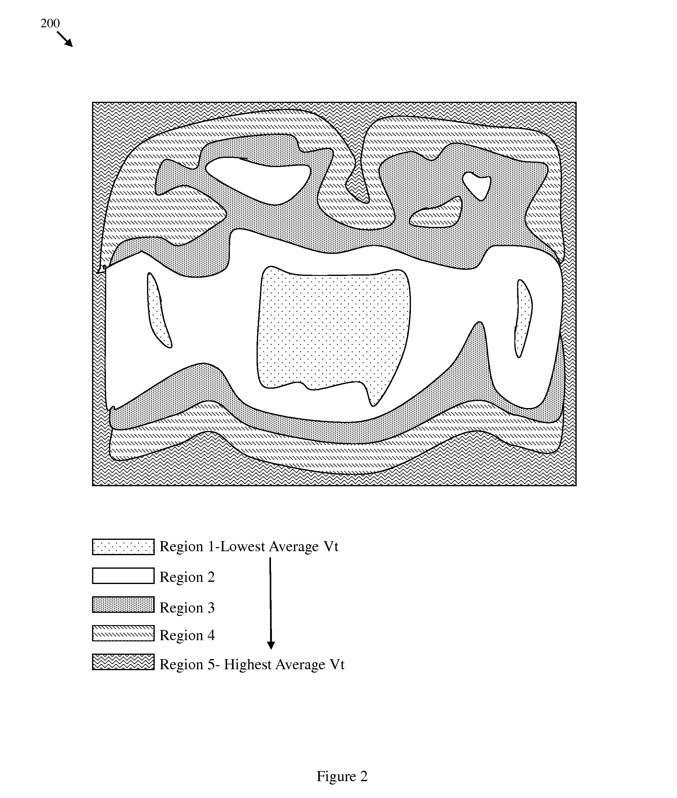
[0017]As mentioned above, circuit limited yield loss refers to the percentage of integrated circuit chips that, when manufactured according to a given design, will not / do not meet pre-defined performance expectations (e.g., clock frequency and power consumption expectations). Across-chip parametric variations (i.e., across-chip variations in a device parameter, such as threshold voltage, effective channel length, sheet resistance, drive current, leakage current, etc.) can cause significant variations in device performance and, thereby can cause circuit limited yield loss. Some across-chip parametric variations may be random. That is, they may be unpredictable. Others may be systematic (i.e., deterministic, predictable, etc.) a...


PUM


Abstract

Disclosed are a system and a method of correcting systematic, design-based, parametric variations on integrated circuit chips to minimize circuit limited yield loss. Processing information and a map of a chip are stored. The processing information can indicate an impact, on a given device parameter, of changes in a value for a specification associated with a given process step. The map can indicate regional variations in the device parameter (e.g., threshold voltage). Based on the processing information and using the map as a guide, different values for the specification are determined, each to be applied in a different region of the integrated circuit chip during the process step in order to offset the mapped regional parametric variations. A process tool can then be selectively controlled to ensure that during chip manufacturing the process step is performed accordingly and, thereby to ensure that the regional parametric variations are minimized.

Description

BACKGROUND[0001]1. Field of the Invention[0002]The embodiments of the invention generally relate to circuit limited yield loss and, more specifically, to a system and an associated method for correcting systematic parametric variations on integrated circuit chips in order to minimize circuit limited yield loss.[0003]2. Description of the Related Art[0004]Circuit limited yield loss refers to the percentage of integrated circuit chips that, when manufactured according to a given design, will not / do not meet pre-defined performance expectations (e.g., clock frequency and power consumption expectations). Across-chip parametric variations (i.e., across-chip variations in device parameters such as threshold voltage, effective channel length, sheet resistance, drive current, leakage current, etc.) can cause significant variations in device performance and, thereby can cause circuit limited yield loss. Some across-chip parametric variations may be random. That is, they may be unpredictable....

Claims


Application Information

Patent Timeline
Patent Type & Authority Applications(United States)
IPC IPC(8): G06F17/50
CPCG06F2217/10G06F17/5068G06F30/39G06F2111/08
Inventor CULP, JAMES A.ELLIS-MONAGHAN, JOHN J.GAMBINO, JEFFREY P.PETERSON, KIRK D.RANKIN, JED H.
Owner GLOBALFOUNDRIES INC
Why Eureka
Try Eureka