Semiconductor apparatus and chip selection method thereof

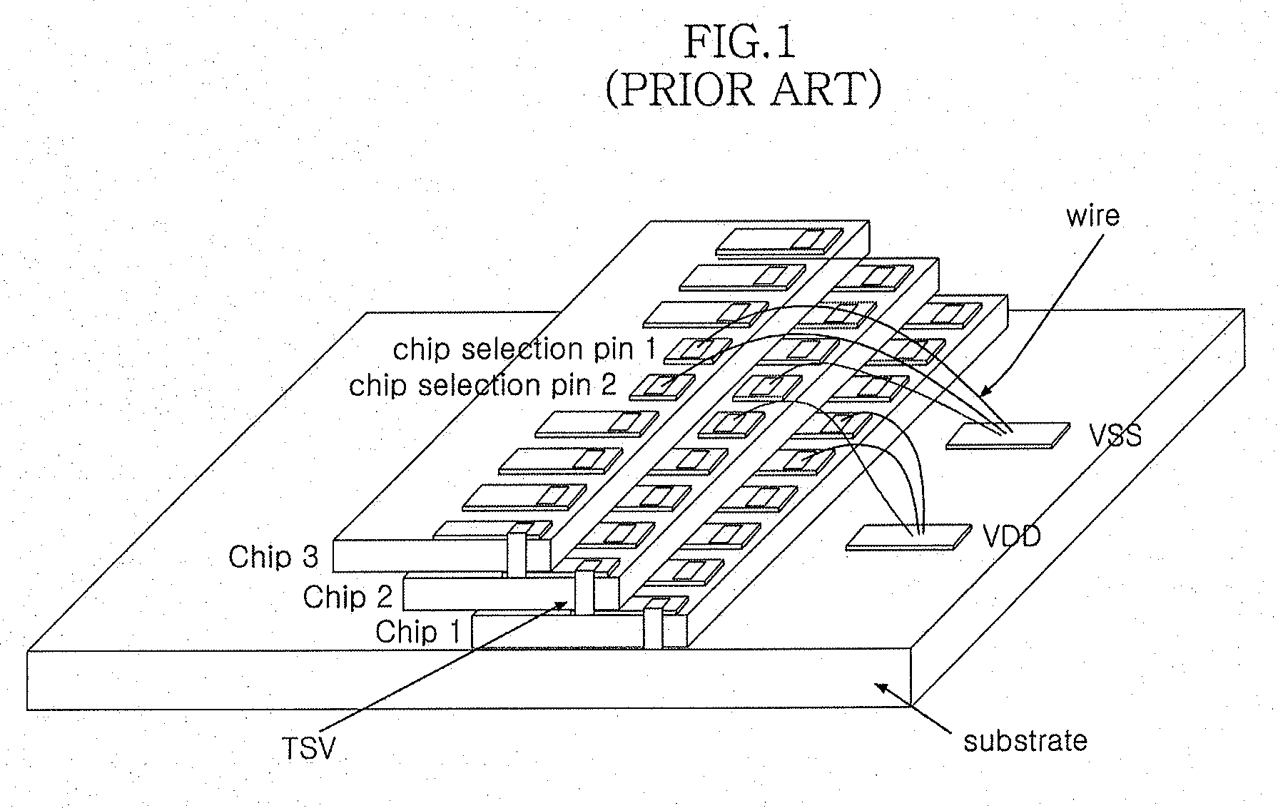
a semiconductor and chip technology, applied in the field of semiconductor apparatuses, can solve the problems of complex wiring structure, limited number of available chip selections, and complicated package structur

Active Publication Date: 2011-05-05
SK HYNIX INC
View PDF17 Cites 18 Cited by
  • Summary
  • Abstract
  • Description
  • Claims
  • Application Information

AI Technical Summary

Benefits of technology

[0008]Accordingly, there is a need for an improved semiconductor memory apparatus and a related chip selection method that may overcome one or more of the problems discussed above. Therefore, various a

Problems solved by technology

However, since the related-art semiconductor apparatus is required to be equipped with separate chip selection pins as described, it is difficult to secure a surface area for the chip selection pins which strictly limits the number of available chip selections.
In addition, since separate wire connections are needed to

Method used


Image

  • Semiconductor apparatus and chip selection method thereof
  • Semiconductor apparatus and chip selection method thereof
  • Semiconductor apparatus and chip selection method thereof

Examples


Embodiment Construction

[0017]Hereinafter, a semiconductor apparatus and a chip selection method thereof, according to the present invention, will be described below with reference to the accompanying drawings through preferred embodiments.

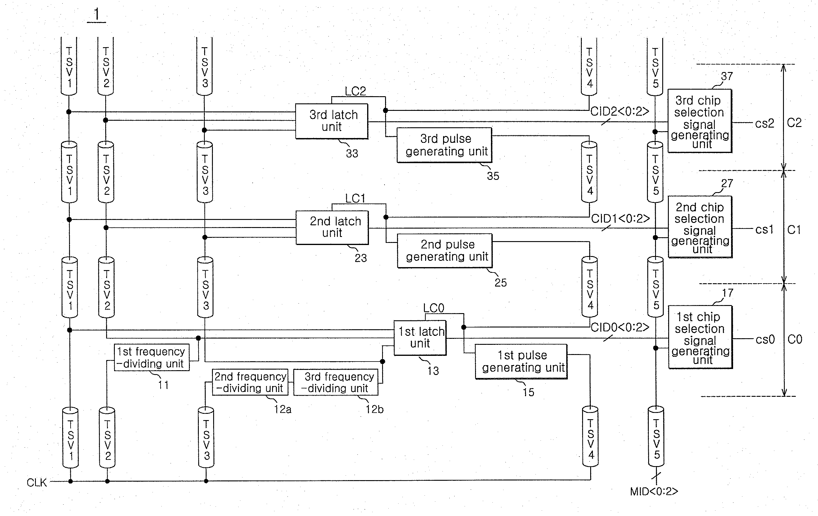
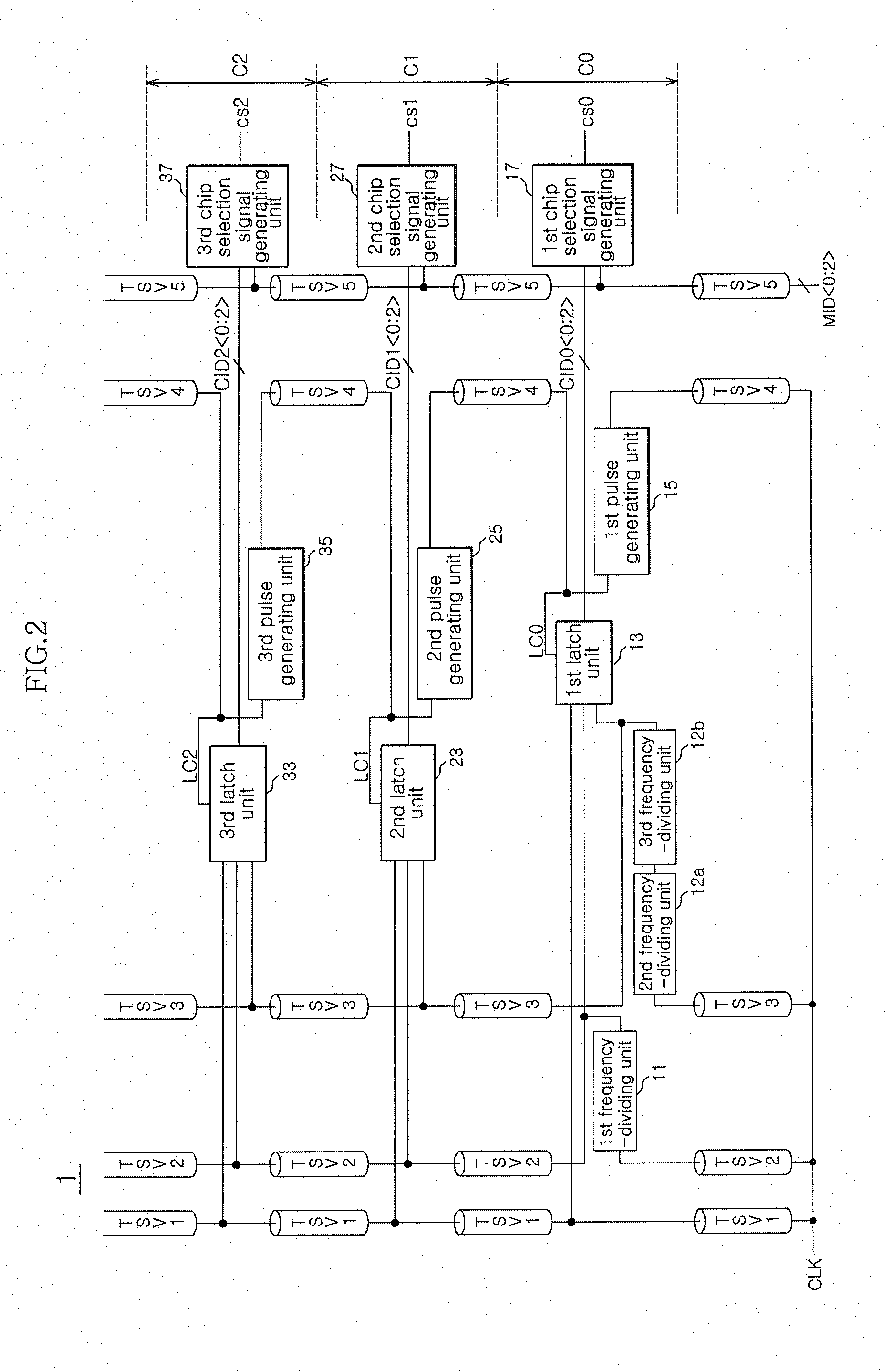
[0018]FIG. 2 is a block diagram schematically showing a configuration of a semiconductor apparatus according to an embodiment of the invention. As shown in FIG. 2, a plurality of chips C0 to C2 are vertically stacked one on top of another to constitute the semiconductor apparatus 1. The plurality of stacked chips C0 to C2 are electrically connected to one another by a plurality of through silicon vias TSV1 to TSV5 penetrating the plurality of chips C0 to C2. In the embodiment, only three chips and only five TSVs are illustrated for convenience of description, but the number of stacked chips and the number of TSVs are not limited thereto, that is, the semiconductor apparatus 1 may include more stacked chips and more TSVs.

[0019]As shown in FIG. 2, the first to third TSVs T...


PUM


Abstract

A semiconductor apparatus having a plurality of stacked chips includes: a plurality of latch units, each of which is disposed in a corresponding one of the plurality of chips and is configured to latch a clock signal and a frequency-divided signal at mutually different points of time to generate an chip identification signal of the corresponding one of the plurality of chips; and a plurality of chip selection signal generating units, each of which is disposed in the corresponding one of the plurality of chips and is configured to compare the chip identification signal of the corresponding one of the plurality of chips with a chip selection identification signal to generate a chip selection signal of the corresponding one of the plurality of chips, wherein the chip selection signal is configured to enable the corresponding one of the plurality of chips when the chip identification signal matches the chip selection identification signal.

Description

CROSS-REFERENCE TO RELATED APPLICATION[0001]The present application claims priority under 35 U.S.C. §119(a) to Korean Application No. 10-2009-0103597, filed on Oct. 29, 2009, which is incorporated by reference in its entirety as if set forth in full.BACKGROUND[0002]1. Technical Field[0003]Various aspects of the present disclosure generally relate to a semiconductor apparatus, and more particularly, to a chip selection method for the semiconductor apparatus.[0004]2. Related Art[0005]In an effort to increase an integration density of a semiconductor apparatus, a three-dimensional (3D) semiconductor apparatus that stacks and packages a plurality of chips into a single package is recently being developed. Since the 3D semiconductor apparatus includes multiple chips in a single device, the 3D semiconductor apparatus is configured such that an electrical signal can distinguish each of the plurality of chips from other chips and select a specific chip from the plurality of chips.[0006]FIG....

Claims


Application Information

Patent Timeline
IPC IPC(8): H03H11/40
CPCG11C5/04H01L24/49H01L25/0657H01L2224/48091H01L2224/49113H01L2924/01006H01L2225/06541H01L2225/06562H01L2924/01033H01L2225/06513H01L2924/00014H01L24/48H01L2224/45099H01L2224/05599G11C8/12G11C7/22G11C7/10
Inventor JIN, SIN HYUNLEE, JONG CHERN
Owner SK HYNIX INC
Why Eureka
Try Eureka