Method for optimizing location and number of power/ground pads on power/ground distribution network with multiple voltage domains

a technology of power/ground pads and voltage domains, applied in the direction of program control, data acquisition and logging, instruments, etc., can solve the problems of increasing the optimization time, wasting unnecessary time, and not being suitable for recent integrated circuit layouts

Active Publication Date: 2011-05-05
ENTASYS DESIGN
View PDF11 Cites 15 Cited by
  • Summary
  • Abstract
  • Description
  • Claims
  • Application Information

AI Technical Summary

Benefits of technology

[0048]In addition, optimized pads can be automaticall

Problems solved by technology

Accordingly, the aforementioned optimization method is not suitable for recent integrated circuit layouts using bump bonding which requires a large number of pads since a long time is taken for the optimization.
However, when the conventional global optimization method is applied to the recent integrated circuit layouts using bum

Method used


Image

  • Method for optimizing location and number of power/ground pads on power/ground distribution network with multiple voltage domains
  • Method for optimizing location and number of power/ground pads on power/ground distribution network with multiple voltage domains
  • Method for optimizing location and number of power/ground pads on power/ground distribution network with multiple voltage domains

Examples


Embodiment Construction

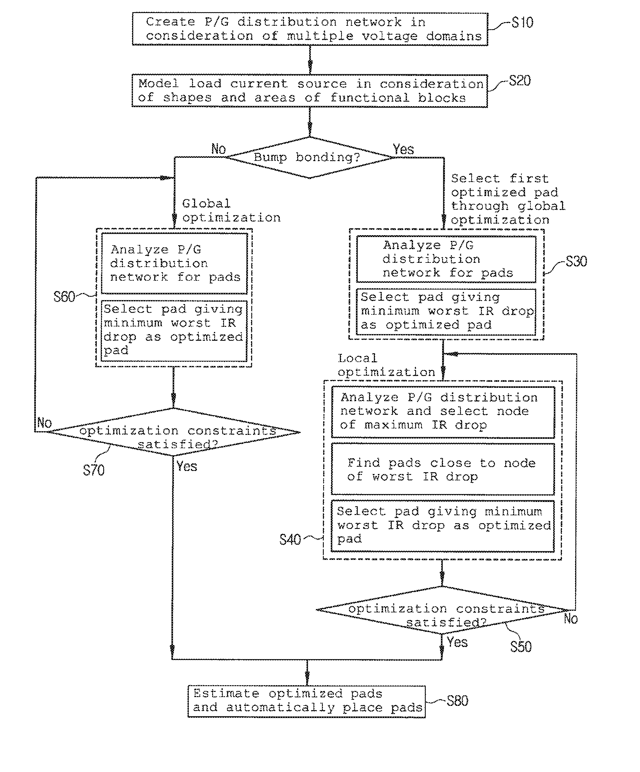
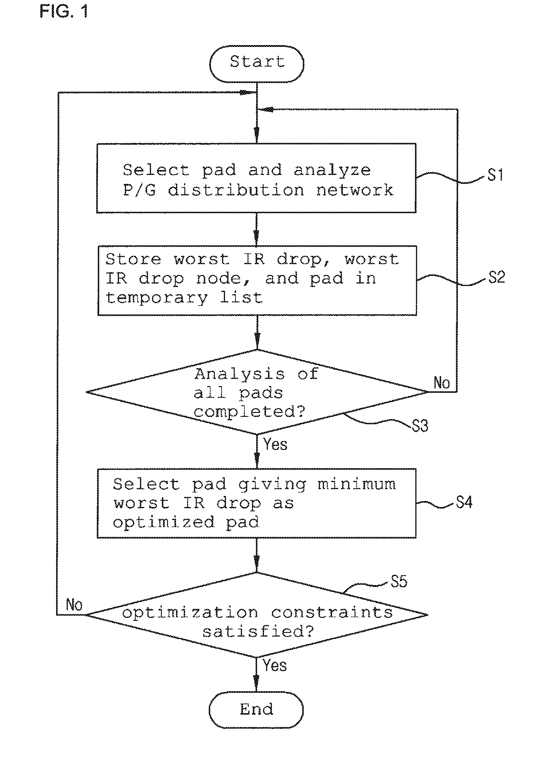
[0059]Hereinafter, the present invention will be described in detail by explaining preferred embodiments of the invention with reference to the attached drawings.

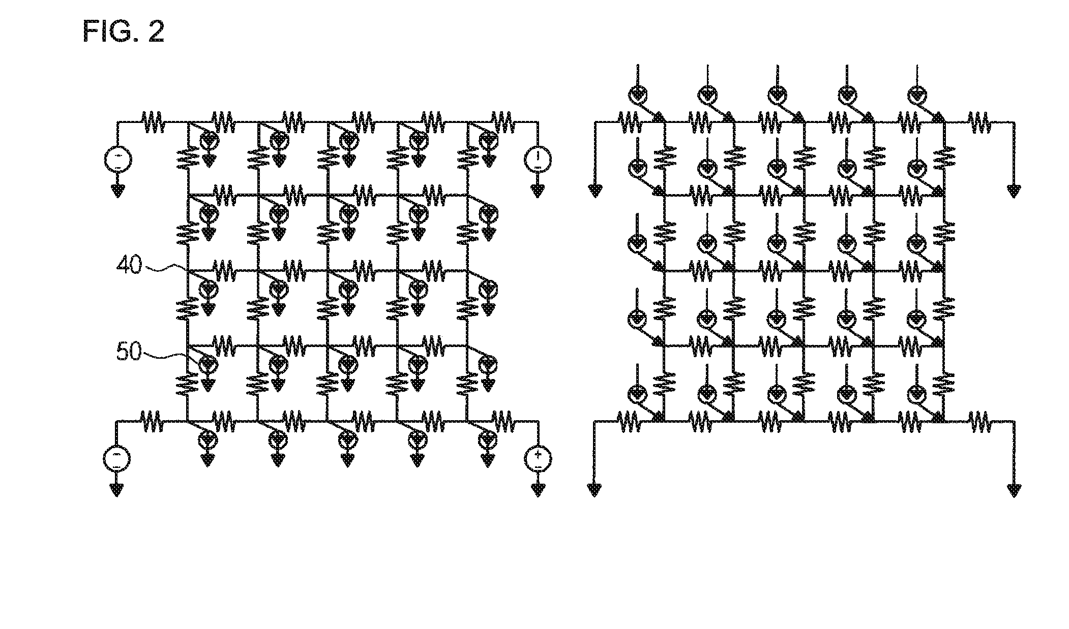
[0060]FIG. 2 illustrates modeling of a power / ground distribution network of a chip and FIG. 3 illustrates multiple voltage domains, basic blocks and pads for explaining the present invention.

[0061]Multiple functional blocks 20 of a chip 1 are classified by voltage domains 10 and pad optimization according to the present invention is performed for each voltage domain 10. FIG. 3 illustrates multiple voltage domains A, B, C and D and bump bonding pads as pads. Although the pad optimization is carried out for each voltage domain 10, the pad optimization is executed for the voltage domain A shown in FIG. 3 as an example in the description. The power / ground distribution network as shown in FIG. 2 is created for the voltage domain A. In the power / ground distribution network, a load current source 50 is applied to each node 40.

[006...


PUM


Abstract

The present invention relates to a method for optimizing power/ground pads in a power/ground distribution network. A power/ground distribution network is created for each of multiple voltage domains and a load current source of each node of the power/ground distribution network is modeled in consideration of the actual shapes and areas of functional blocks. A local optimization method is developed to solve problems generated when a conventional optimization method is applied to optimization of power/ground pads in a bump shape used for a flip chip, and a combination of global optimization and local optimization is applied to layouts using bump bonding, which is discriminated from the conventional optimization method restrictively applicable to layouts using wire bonding.

Description

BACKGROUND OF THE INVENTION[0001]1. Field of the Invention[0002]The present invention relates to a method for optimizing the location and number of power / ground pads on a power / ground distribution network with multiple voltage domains. More specifically, the invention relates to a method for decreasing an optimization time and securing the minimum number and location of pads in a power distribution network layout by solving problems generated when a conventional pad optimization method is applied to a power / ground distribution network layout using bump bonding and supplementing shortcomings of the conventional pad optimization method.[0003]2. Background of the Related Art[0004]It is very important to provide power to functional blocks constituting an integrated circuit while decreasing IR drop generated in a power / ground distribution network of the integrated circuit below a reference value. This can be achieved by determining the optimized location and number of power / ground pads t...

Claims


Application Information

Patent Timeline
IPC IPC(8): G06F17/50G06F17/40
CPCG06F17/5068G06F2217/78Y02E60/76Y04S10/545Y04S40/22Y02E40/76G06F30/39G06F2119/06Y02E40/70Y02E60/00Y04S10/50Y04S40/20
Inventor OH, SUNG HWANSHIN, DONG JIN
Owner ENTASYS DESIGN
Why Eureka
Try Eureka