MEMS device

a technology of a device and a chip, applied in the direction of instruments, semiconductor electrostatic transducers, acceleration measurement using interia forces, etc., can solve the problem of high cost due to the use of ceramic packages b>202/b>, and achieve the effect of high cos

Inactive Publication Date: 2011-05-12
ROHM CO LTD
View PDF2 Cites 48 Cited by
  • Summary
  • Abstract
  • Description
  • Claims
  • Application Information

AI Technical Summary

Benefits of technology

[0039]With the conventional acceleration sensor 201, the cavity for sealing the sensor chip 204 and the circuit chip 205 is arranged by closing the ho

Problems solved by technology

However, there is an issue of high cost due to us

Method used


Image

  • MEMS device
  • MEMS device
  • MEMS device

Examples


Embodiment Construction

[0099]Preferred embodiments of the present invention shall now be described in detail with reference to the drawings.

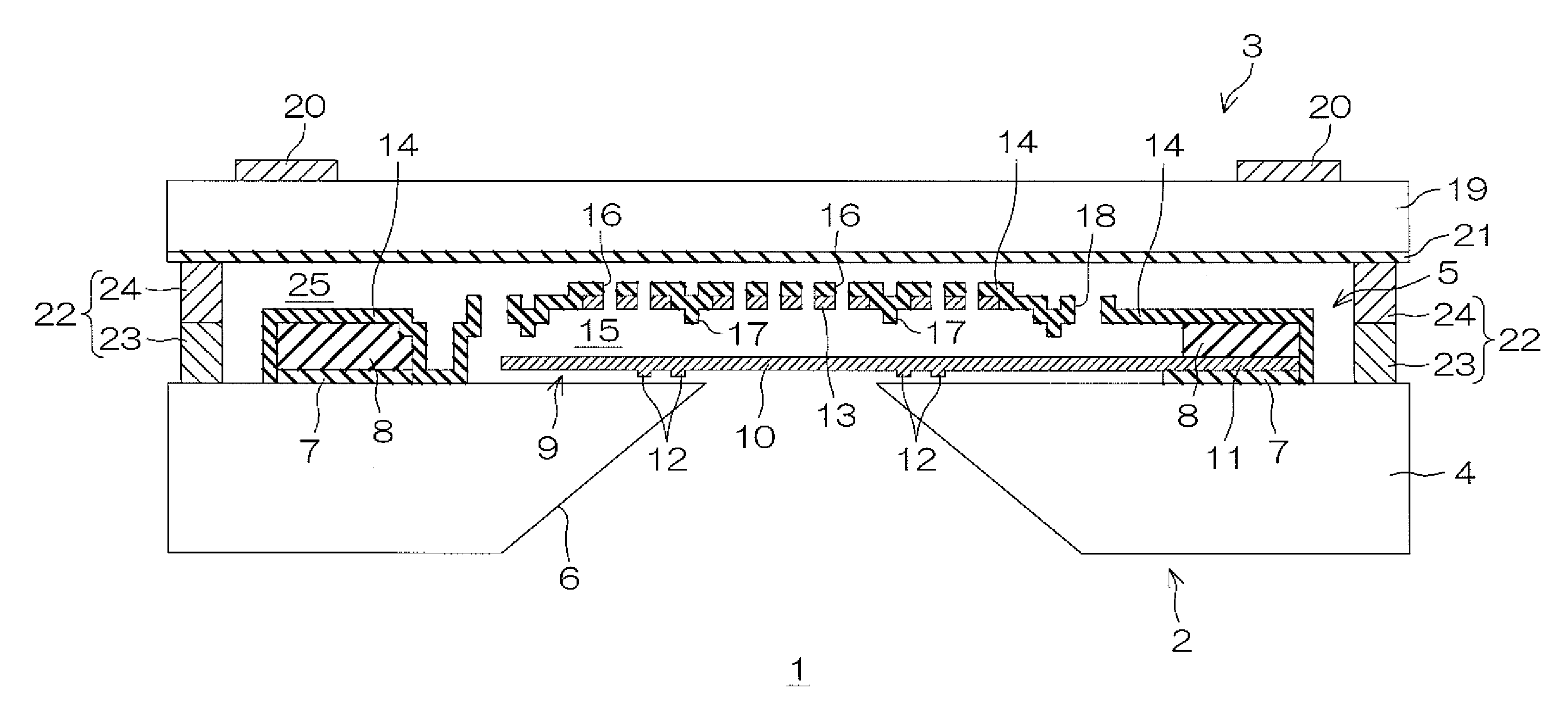
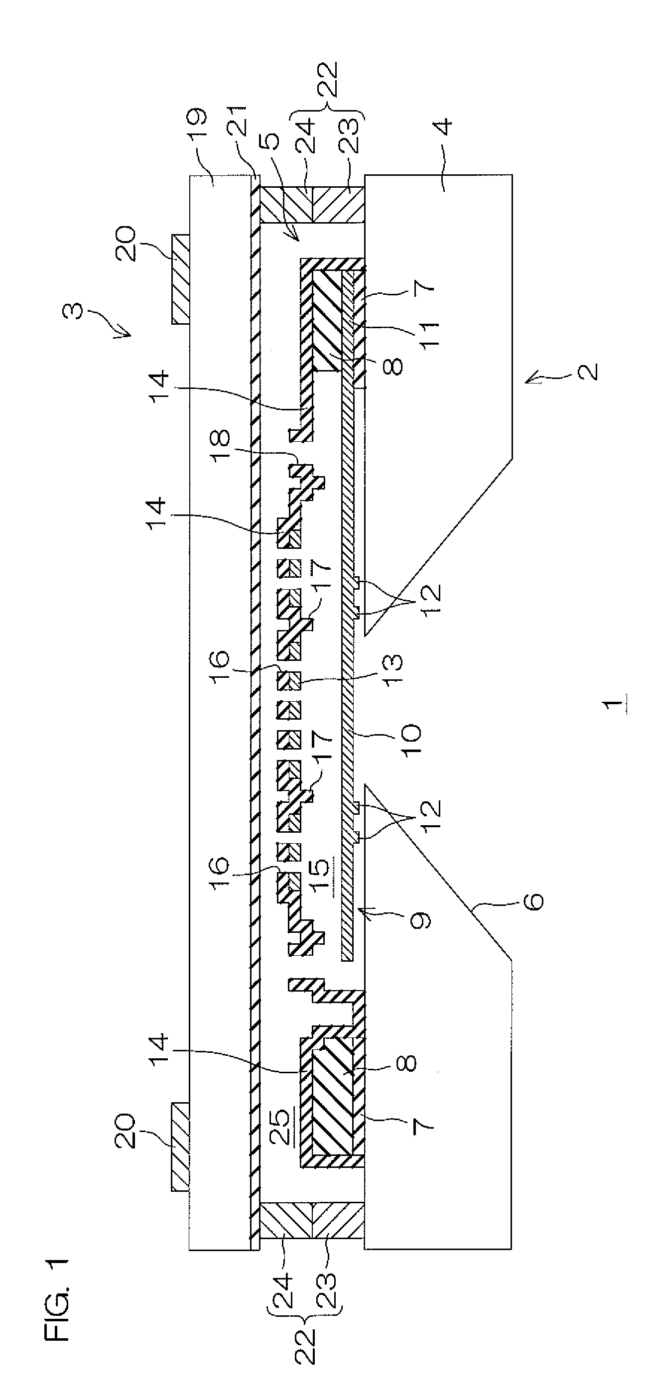
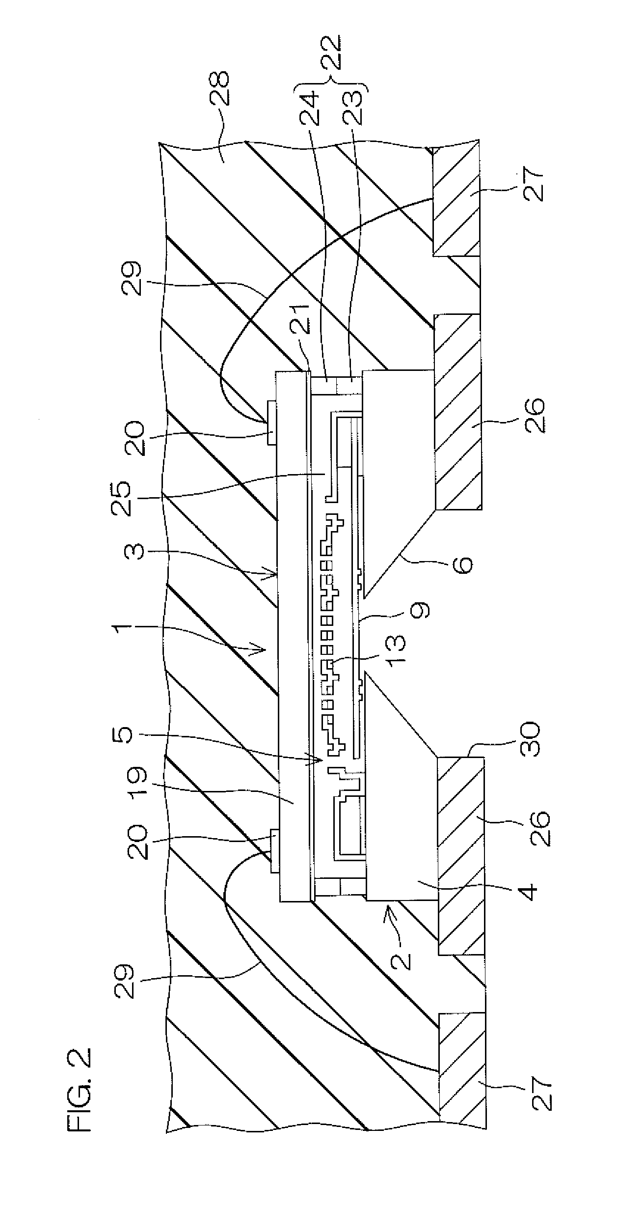
[0100]FIG. 1 is a schematic sectional view of a principal portion of a silicon microphone according to a first preferred embodiment of the present invention.

[0101]The silicon microphone includes a device chip 1.

[0102]The device chip 1 includes a microphone chip 2 and a circuit chip 3 opposed to the microphone chip 2 and has a chip-on-chip structure in which the chips are bonded overlappingly.

[0103]The microphone chip 2 is a chip manufactured by MEMS technology and includes a supporting substrate 4 made of silicon and a movable device portion 5 supported by the supporting substrate 4 and outputting an audio signal generated by a vibrational movement of a movable body.

[0104]The supporting substrate 4 is formed to a rectangular shape in plan view. A through hole 6 of trapezoidal cross-sectional shape that narrows toward a top surface side (widens toward a rear surface si...


PUM


Abstract

A MEMS device according to the present invention includes a movable member, a supporting member supporting the movable member, an opposing member opposed to the movable member, and a wall member formed to an annular shape surrounding the movable member and connected to the supporting member and the opposing member.

Description

FIELD OF THE ART[0001]The present invention relates to various devices manufactured by MEMS (Micro Electro Mechanical Systems) technology.BACKGROUND ART[0002]Recently, MEMS devices have been drawing rapidly increasing attention due to MEMS devices being installed in cell phones, etc. Representative examples of MEMS devices include acceleration sensors and silicon microphones.[0003]An acceleration sensor includes, for example, a weight that oscillates due to an action of acceleration and a membrane that deforms in linkage with the oscillation of the weight. The membrane is provided with a piezoresistor. The membrane deforms due to the oscillation of the weight, and a stress acts on the piezoresistor provided in the membrane. The piezoresistor thereby changes in resistivity and an amount of change of the resistivity is output as a signal.[0004]Meanwhile, a silicon microphone includes, for example, a diaphragm (vibrating plate) that vibrates due to an action of sound pressure (sound wa...

Claims


Application Information

Patent Timeline
IPC IPC(8): H01L29/84G01P15/18
CPCB81B2201/0235B81B2201/0242H01L2924/1461H01L2224/48247H01L2224/48091B81B2201/0257B81B2201/0264B81C1/00238B81C2203/0109B81C2203/019G01P1/023G01P15/0802G01P15/123H01L28/40H04R19/005H04R19/04H04R2499/11H01L2924/00014H01L2924/00
Inventor NAKATANI, GORO
Owner ROHM CO LTD
Why Eureka
Try Eureka