
Processing method for soi substrate

a processing method and substrate technology, applied in biomass after-treatment, specific use bioreactors/fermenters, biochemistry apparatus and processes, etc., can solve the problems of misalignment of contact surfaces between the three plates, non-uniform wafer sectional profile, etc., and achieve stable profile

Inactive Publication Date: 2011-05-12
SAMSUNG ELECTRO MECHANICS CO LTD
View PDF2 Cites 0 Cited by
  • Summary
  • Abstract
  • Description
  • Claims
  • Application Information

AI Technical Summary

Benefits of technology

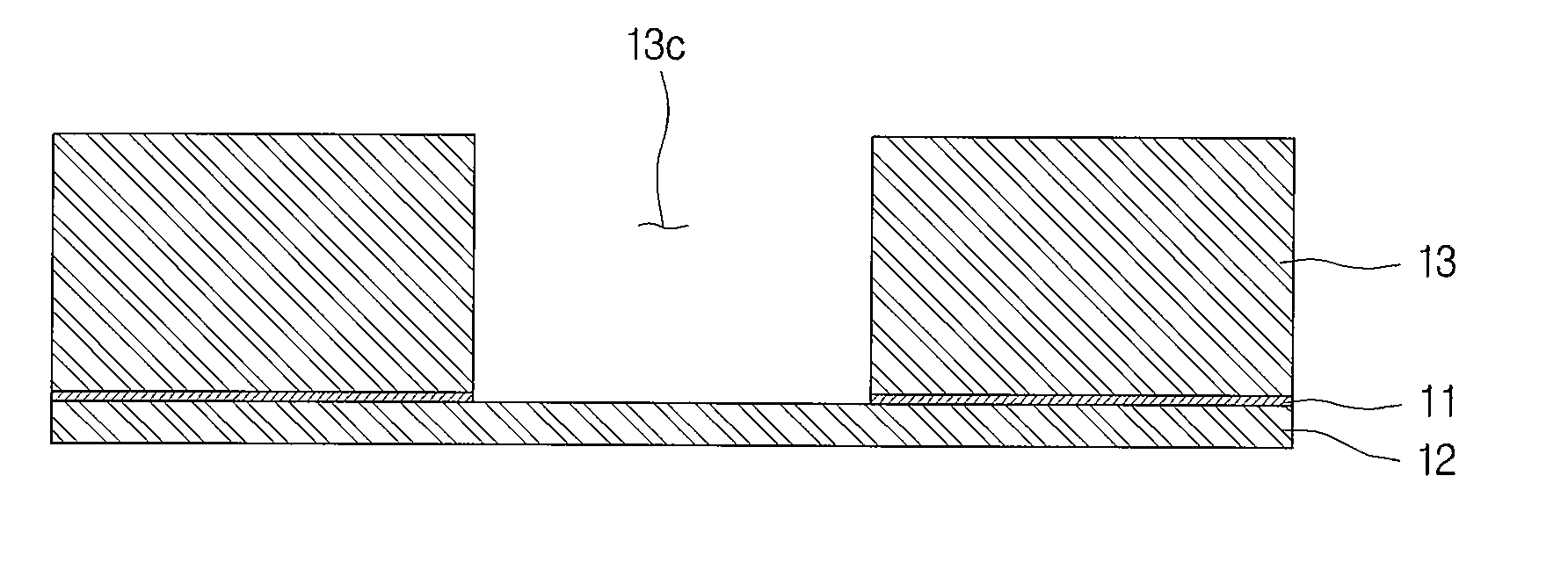
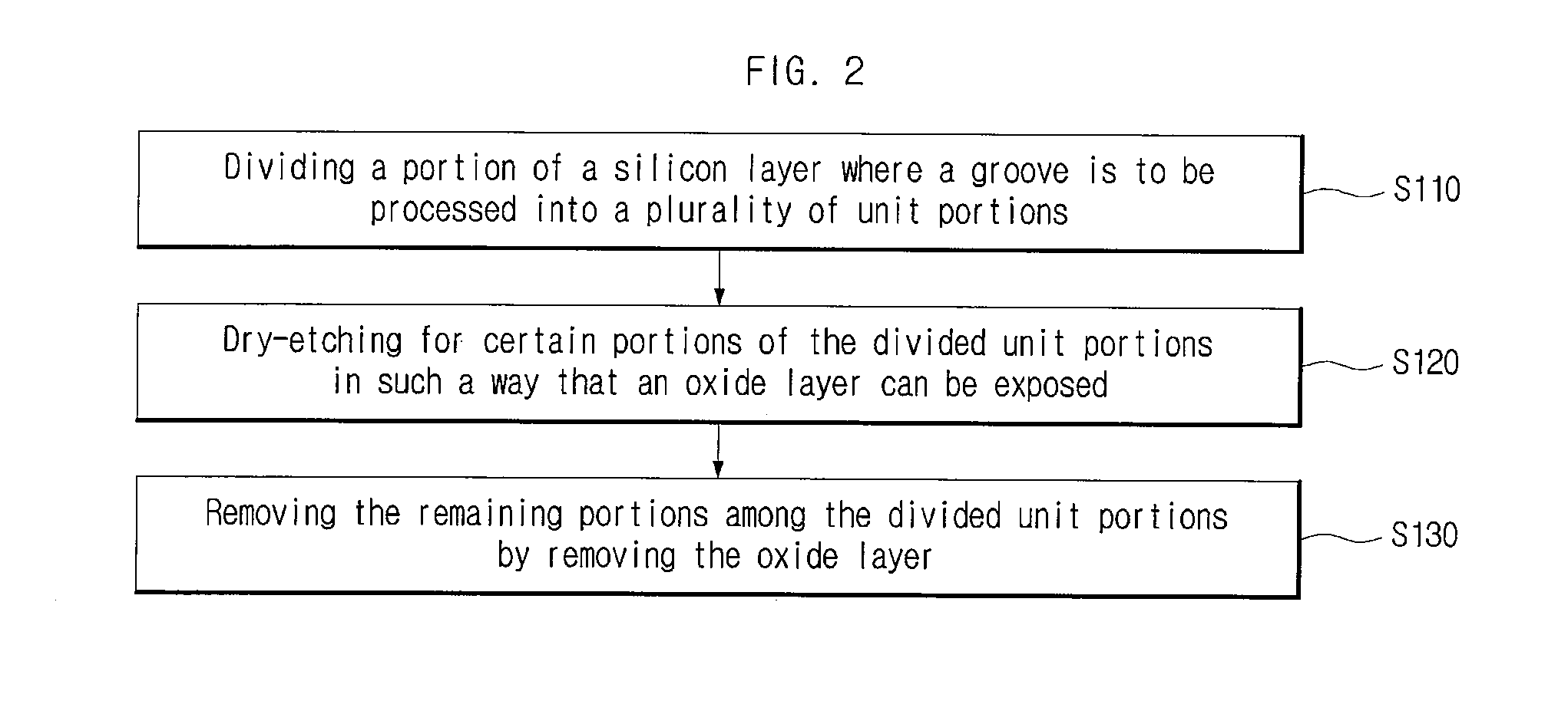
The present invention provides a method for processing an SOI substrate to form a groove in the substrate. This method can secure a stable profile even when a large area of the substrate is processed. The method includes dividing a portion of the silicon layer in which the groove is to be processed into multiple unit portions, performing dry etching on certain portions of the divided unit portions to expose the oxide layer, and removing remaining portions of the divided unit portions by removing the oxide layer. This method can be used in the manufacturing of inkjet heads, where the groove can serve as a reservoir, pressure chamber, or ink channel. The removal of remaining portions can be performed using wet etching. The technical effects of this invention include achieving a stable profile when processing a large area of the substrate and improving the manufacturing of inkjet heads.

Problems solved by technology

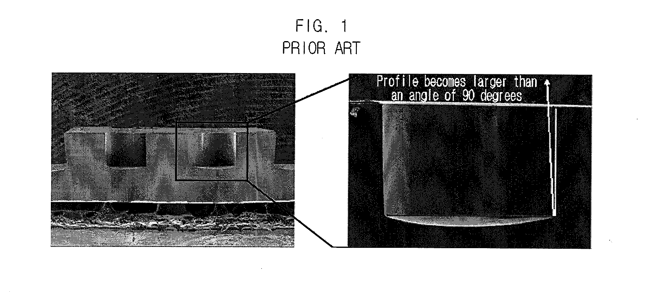
However, if a channel having a large area is formed by using a reactive ion etching (RIE) device, a sectional profile in the wafer becomes non-uniform after performing an etching process.
In other words, the shape actually processed is different from the originally designed shape, and thus if an inkjet head is completed by coupling top, middle and bottom plates to one another, the contact surfaces between the three plates may be misaligned.

Method used


Image

  • Processing method for soi substrate
  • Processing method for soi substrate
  • Processing method for soi substrate

Examples


Embodiment Construction

[0018]As the invention allows for various changes and numerous embodiments, a particular embodiment will be illustrated in the drawings and described in detail in the written description. However, this is not intended to limit the present invention to a particular mode of practice, and it is to be appreciated that all changes, equivalents, and substitutes that do not depart from the spirit and technical scope of the present invention are encompassed in the present invention. In the description of the present invention, certain detailed explanations of related art are omitted when it is deemed that they may unnecessarily obscure the essence of the invention.

[0019]A method of processing an SOI substrate in accordance with a certain embodiment of the present invention will be described in more detail through the below description with reference to the accompanying drawings. Those components that are the same or are in correspondence are rendered the same reference numeral regardless of...


PUM

PropertyMeasurementUnit
angleaaaaaaaaaa
shapeaaaaaaaaaa
pressureaaaaaaaaaa

Abstract

A method of processing a SOI substrate to form a groove in the SOI substrate in which a silicon layer is stacked on both sides of an oxide layer is disclosed. In accordance with an embodiment of the present invention, the method includes dividing a portion of the silicon layer, in which the groove is to be processed, into a plurality of unit portions, performing dry etching on certain portions of the plurality of divided unit portions such that the oxide layer is exposed and removing remaining portions of the plurality of divided unit portions by removing the oxide layer.

Description

CROSS-REFERENCE TO RELATED APPLICATIONS[0001]This application claims the benefit of Korean Patent Application No. 10-2009-0109052, filed with the Korean Intellectual Property Office on Nov. 12, 2009, the disclosure of which is incorporated herein by reference in its entirety.BACKGROUND[0002]1. Technical Field[0003]The present invention is related to a method of processing an SOI substrate.[0004]2. Description of the Related Art[0005]If a MEMS process is used to manufacture an inkjet head, it is needed to form a layer including an ink channel. The ink channel takes up a relatively large portion of a silicon wafer. To form the ink channel in the silicon wafer, a deep reactive ion etching (DRIE) method is widely used.[0006]However, if a channel having a large area is formed by using a reactive ion etching (RIE) device, a sectional profile in the wafer becomes non-uniform after performing an etching process. That is, as illustrated in FIG. 1, the pattern processed in a middle plate of t...

Claims


Application Information

Patent Timeline
Patent Type & Authority Applications(United States)
IPC IPC(8): H01L21/306
CPCB41J2/1603B41J2/1631B41J2/1628B41J2/04B41J2/16C23F1/02
Inventor YANG, CHUNG-MOJOUNG, JAE-WOOYOO, YOUNG-SEUCK
Owner SAMSUNG ELECTRO MECHANICS CO LTD
Learn More