Eureka AIR delivers breakthrough ideas for toughest innovation challenges, trusted by R&D personnel around the world.

Electronic device and flat display module

Inactive Publication Date: 2011-05-12
SONY MOBILE COMM INC
View PDF6 Cites 12 Cited by
  • Summary
  • Abstract
  • Description
  • Claims
  • Application Information

AI Technical Summary

Benefits of technology

[0009]It is desirable to prepare the ESD measure with respect to a flat display module while eliminating restriction to a mechanism structure of the electronic device as much as possible.
[0011]According to the construction, ESD entering into the case body from outside is captured on the conductive layer and electrically connected to GND of the circuit board by the ground means. Therefore, ESD is prevented from entering to the electrode which is exposed on the surrounding side of the flat display module.
[0014]The ground means may be constructed of the conductive member having elasticity. By doing this, it may be possible to guarantee an electrical contact with pressure force when assembling the electronic device.
[0015]Preferably, the conductive foil is deposited on the conductive layer, and the conductive member is contacted with the conductive layer through the conductive foil. By doing this, the conductive layer is protected from destruction caused by ESD even though it is an extremely thin sheet.
[0019]According to the embodiment of the invention, it is desirable to prepare the ESD measure with respect to a flat display module while eliminating restriction to a mechanism structure of the electronic device as much as possible, and accordingly, malfunction or destruction of components may be prevented without restricting minimization of the device.

Problems solved by technology

Use of the vessel or frame is against this request and is a severe hindrance to the minimization of the terminal.
Since the technology described in the JP-A-2008-130912 demands a holding portion to accommodate and hold electronic components in an internal side of the case body, a restriction occurs in its mechanism structure and it is difficult to apply the technology to ESD with respect to a liquid crystal module.

Method used


Image

  • Electronic device and flat display module
  • Electronic device and flat display module
  • Electronic device and flat display module

Examples


Embodiment Construction

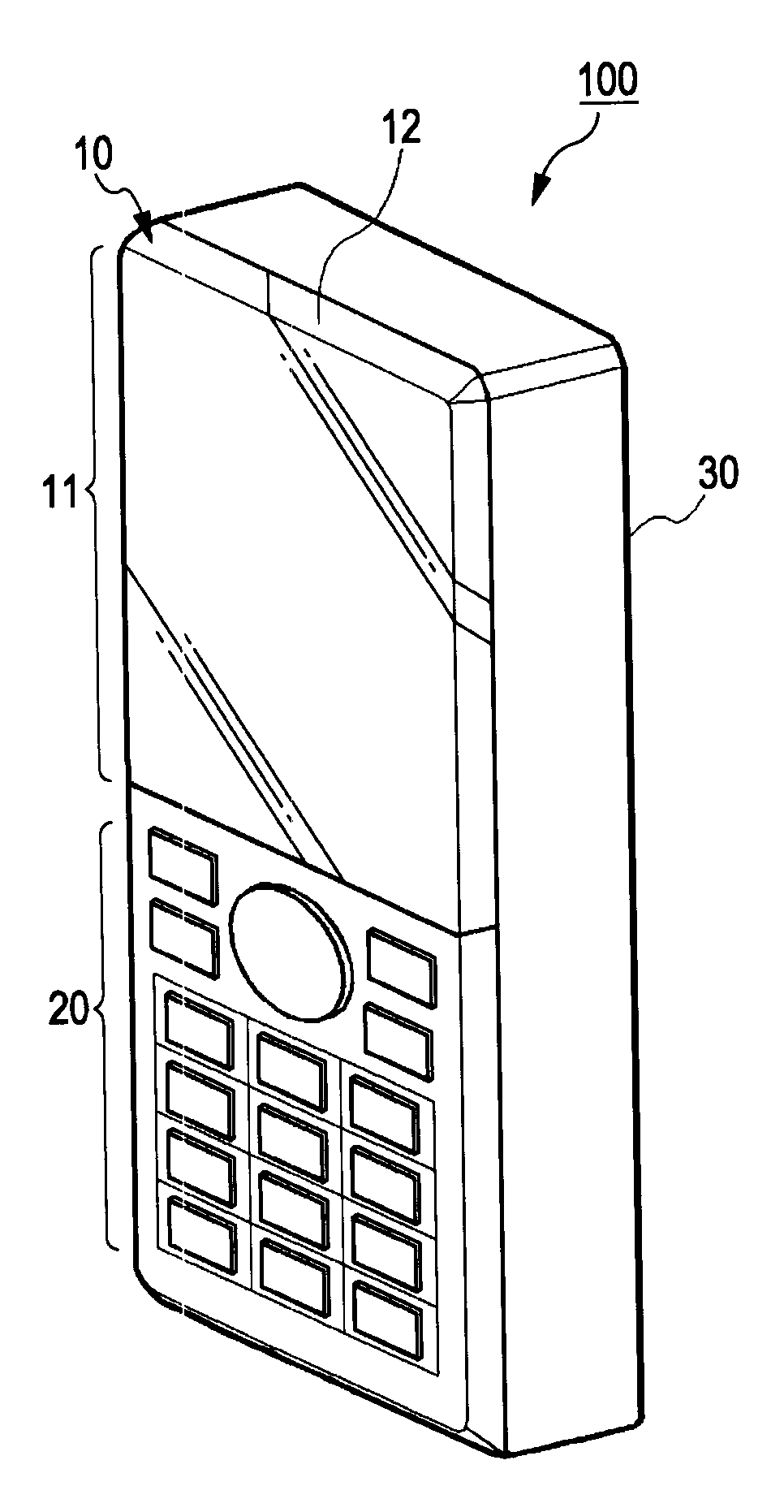
[0030]Hereinafter, a preferred embodiment of the invention will be described with reference to the accompanying drawings. A liquid crystal module is described as an example of a flat display module. A liquid crystal panel is used as an example of a flat display panel constituting a flat display module.

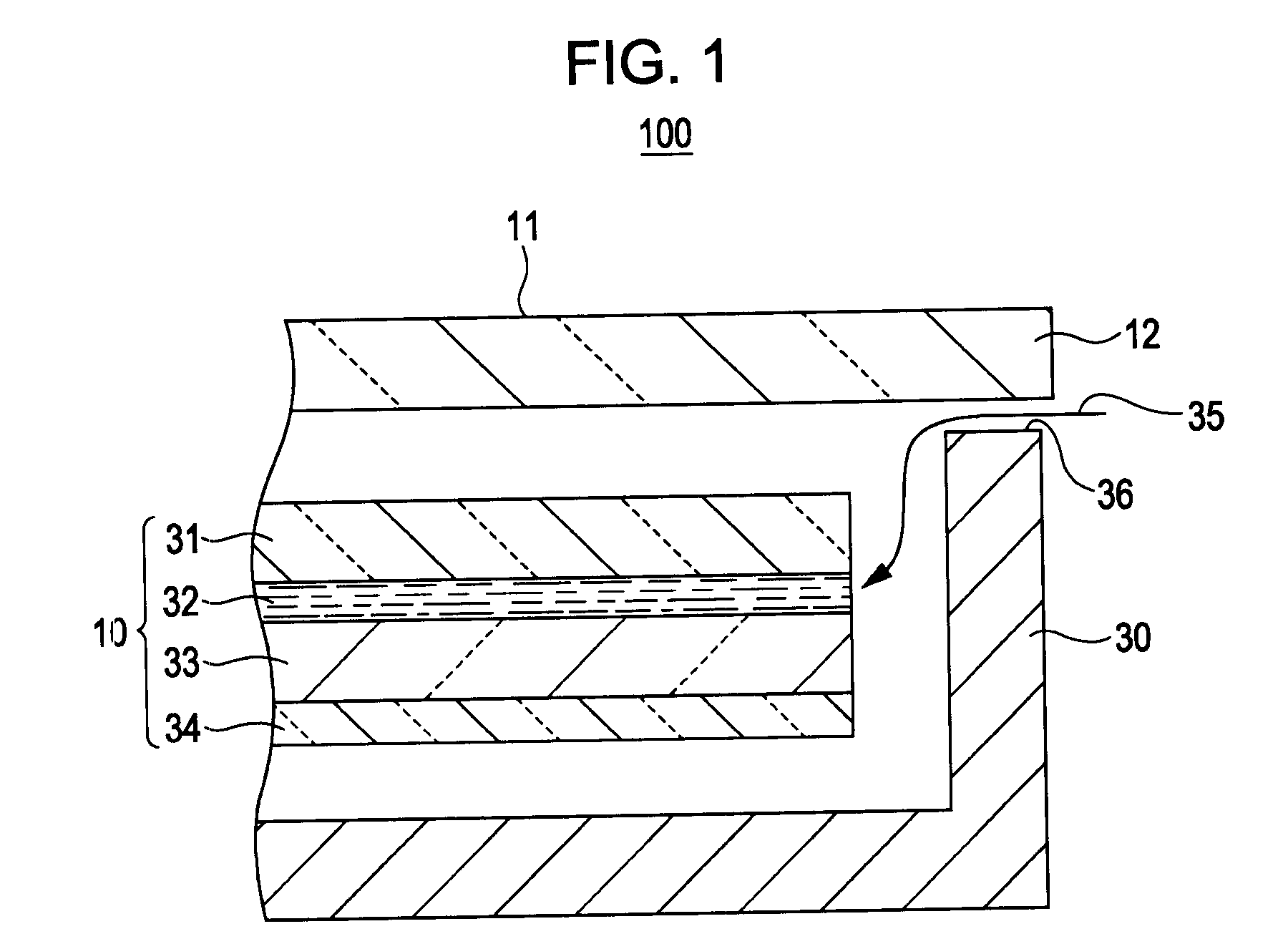
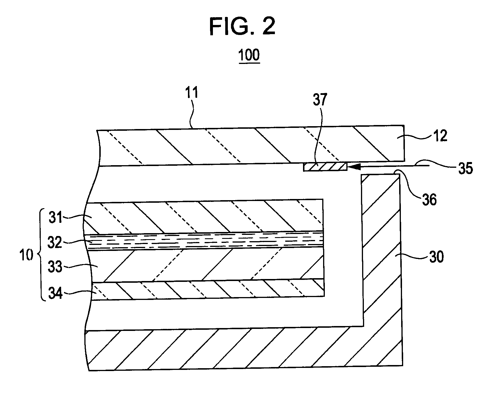
[0031]FIG. 1 is a sectional diagram illustrating a main portion of electronic device having a general liquid crystal display (LCD) mounted therein.

[0032]As illustrated in the drawing, generally, a liquid crystal panel constructing LCD becomes a liquid crystal module that has an electronic circuit to provide image signals and driving power and an optical source for backlight attached thereon as a unit and is accommodated in a case body. The case body is assembled by overlapping a front side portion 12 of the case body and a rear side portion 30 of the case body. Accordingly, a gap 36 inevitably occurs at a contact portion of the portions of the case body, and it becomes an ESD entry pat...


PUM


Abstract

Disclosed is electronic device including a case body including a front surface side portion of the case body and a rear surface side portion of the case body; a flat display module accommodated in the case body; a conductive layer formed on an internal wall of one of the front surface side portion of the case body and the rear surface side portion of the case body, the internal wall being around a contact portion of both portions of the case body; a circuit board having electrical components mounted thereon; and a ground means that electrically connects the conductive layer to a GND of the circuit board.

Description

BACKGROUND OF THE INVENTION[0001]1. Field of the Invention[0002]The present invention relates to electronic device whose representative is a mobile phone terminal and a flat display module used for the same.[0003]2. Description of the Related Art[0004]Recently, a mobile terminal having a flat display using a flat display panel mounted thereon is widely used, which is a representative of liquid crystal display (LCD). In this situation, it is important to prepare measures for electrostatic discharge (ESD) with respect to the flat display module as a component having the flat display panel mounted therein in order to guarantee quality and reliability of products.[0005]For example, in the case of the liquid crystal module, a transparent electrode constructed of ITO (Indium Tin Oxide) and the like is exposed on its surrounding side, and a liquid crystal driving circuit to drive the liquid crystal module and the like are arranged on the side of the display unit. When the ESD enters into t...

Claims


Application Information

Patent Timeline
IPC IPC(8): H04W88/02G09G3/34G02F1/1333G09F9/00H04M1/02H05K9/00
CPCG02F1/133308G02F2001/133334H05K9/0039H04M1/0266H05K9/002G02F2202/22G02F1/133334
Inventor KIDO, NOBUHIKO
Owner SONY MOBILE COMM INC
Why Eureka
Eureka Blog
Learn More