Transmission apparatus

Inactive Publication Date: 2008-01-17
FUJITSU LTD
8 Cites 0 Cited by

AI-Extracted Technical Summary

Problems solved by technology

As a result, the circuit scale and the power consumption will increase considerably if all of the monitor control information is to be sent to the monitor control part 3.
However, if an unimaginable problem that is outside the design range occurs at an evaluating stage where the actual main signal processing device 4 of the optical transmission apparatus 1 that is being ...

Benefits of technology

[0021]Another and more specific object of the present invention is to provide a transmission apparatus which can eliminate the restrictions on the regions of the main signal processing device that are accessible, and facilitate the debugging of the main signal processing device.
[0022]Still another object of the present invention is to provide a transmission apparatus comprising a main signal processing device configured to carry out a main signal processing; a monitor control part configured to set data to the main signal processing device and monitor and control the main signal processing device by reading the data from the main signal processing device in a normal operation mode, and to debug the main signal processing device in a debug mode; an intermediating part configured to intermediate addresses and data between the monitor control part and the main signal processing device; a ...

Abstract

A transmission apparatus has a main signal processing device, a monitor control part and an intermediating part to intermediate addresses and data between the monitor control part and the main signal processing device. The transmission apparatus further has a first switching part to selectively supply the address or the address and the data output from the intermediating part to the main signal processing device in the normal operation mode, and to selectively supply the address or the address and the data output from the monitor control part to the main signal processing device in the debug mode, and a second selecting part to selectively supply the data output from the intermediating part to the monitor control part in the normal operation mode, and to selectively supply the data output from the main signal processing device to the monitor control part in the debug mode.

Application Domain

Technology Topic

Heat outputComputer hardware +2

Image

  • Transmission apparatus
  • Transmission apparatus
  • Transmission apparatus

Examples

  • Experimental program(1)

Example

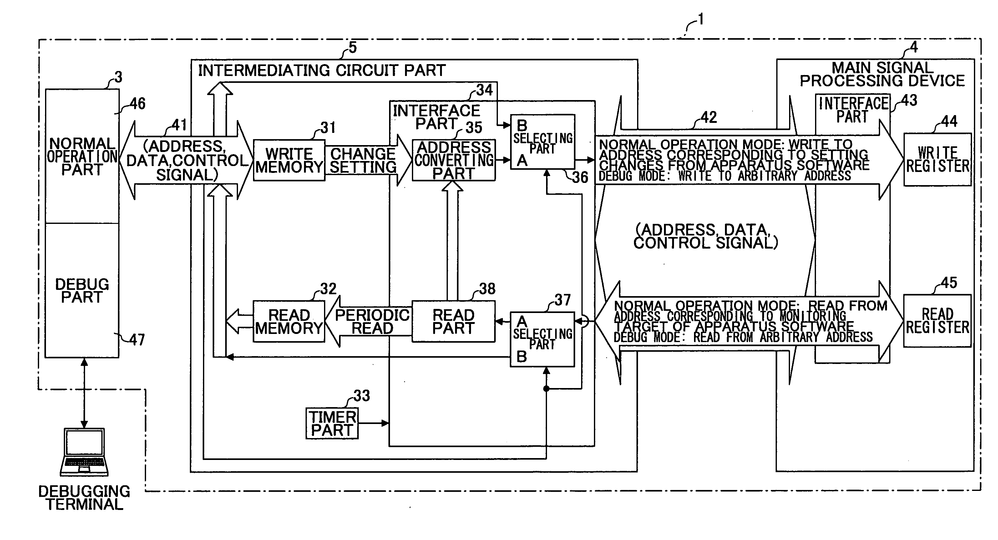
[0029]A description will be given of an embodiment of a transmission apparatus according to the present invention, by referring to FIGS. 4 and 5.
[Structure of the Present Invention]
[0030]FIG. 4 is a system block diagram showing this embodiment of the transmission apparatus according to the present invention. An optical transmission apparatus 1 shown in FIG. 4 has a monitor control part 3, a main signal processing device 4 and an intermediating circuit part 5. The intermediating circuit part 5 has a write memory 31, a read memory 32, a timer part 33, and an interface part 34. An address converting part 35, selecting parts 36 and 37, and a read part 38 are provided within the interface part 34.
[0031]On the other hand, an interface part 43, a write register 44, and a read register 34 are provided within the main signal processing device 4. The monitor control part 3 has a normal operation part 46 and a debug part 47.
[Normal Operation Mode]
[0032]In the normal operation mode, the set data and the logical address are written irregularly from the normal operation part 46 of the monitor control part 3 to the write memory 31 within the intermediating circuit part 5 via an external bus 41.
[0033]The set data and the logical address are read from the write memory 31 at a periodic timing determined by the timer part 33, and are supplied to the interface part 34. The address converting part 35 within the interface part 34 converts the logical address into the physical address of the main signal processing device 4, and supplies the set data and the physical address to an input part A of the selecting part 36.
[0034]An input part B of the selecting part 36 is connected to a data bus and an address bus of the external bus 41. The selecting part 36 also receives a mode control signal from a control line of the external bus 41. The mode control signal instructs the normal operation mode or the debug mode. The selecting part 36 selectively outputs the data and the address received by the input part A when the mode control signal indicates the normal operation mode, and selectively outputs the data and the address received by the input part B when the mode control signal indicates the debug mode.
[0035]In the normal operation mode, the set data and the physical address received via the address converting part 35 are obtained from the selecting part 36, and are supplied to the main signal processing device 4 via an internal bus 42. Hence, the set data is written from the interface part 43 within the main signal processing device 4 to a region of the write register 44 specified by the physical address. For example, the set data includes cross-connect information, band information or the like.
[0036]In addition, in the normal operation mode, the read part 38 within the interface part 34 generates a read logical address at a periodic timing determined by the timer part 33, and supplies the read logical address to the address converting part 35. The read logical address is converted into a physical address of the main signal processing device 4 by the address converting part 35, and is thereafter supplied from the selecting part 36 to the main signal processing device 4 via the internal bus 42. Hence, the state data are read from a region of a read register 45 specified by the physical address. For example, the state data includes monitor information obtained from the overhead such as the SOH (Section OverHead) and the LOH (Lime OverHead), operation state information related to an operating state of the main signal processing device 4, and the like. Therefore, the read state data are supplied from the interface part 43 to the selecting part 37 within the interface part 34.
[0037]An output part A of the selecting part 37 is connected to the read part 38. On the other hand, an output part B of the selecting part 37 is connected to the data bus of the external bus 41. The selecting part 37 also receives the mode control signal from the control line of the external bus 41. The selecting part 37 selectively outputs the data from the output part A when the mode,control signal indicates the normal operation mode, and selectively outputs the data from the output part B when the mode control signal indicates the debug mode.
[0038]For this reason, in the normal operation mode, the state data are supplied from the selecting part 37 to the read part 38, and are written to the read memory 32 from the read part 38. The state data held in the read memory 32 are read irregularly from the monitor control part 3.
[0039]FIG. 5 is a timing chart for explaining a state data read operation and a set data write operation of this embodiment of the transmission apparatus. The mode control signal shown in FIG. 5(D) indicates the normal operation mode by the low-level period thereof, and indicates the debug mode by the high-level period thereof.
[0040]The timer part 33 generates a timing signal shown in FIG. 5(A) at a constant period of 100 milliseconds, for example. In the normal operation mode, the read part 38 makes a read access to the read register 45 at timings indicated by “R” in FIG. 5(B), in response to the timing signal. In addition, the set data from the write memory 31 is written by a write access to the write register 44 at timings immediately after the read access, as indicated by “W” in FIG. 5(B).
[0041]In the normal operation mode, the normal operation part 46 of the monitor control part 3 reads the state data from the read memory 32 for every 1 second, for example, as shown in FIG. 5(C), asynchronously to the timing signal shown in FIG. 5(A). In addition, the normal operation part 46 writes the set data and the write logical address to the write memory 31 if necessary.
[Debug Mode]
[0042]In the debug mode, the debug part 47 of the monitor control part 3 outputs the read physical address or the write physical address and the debug data. The debug part 47 outputs the physical address and not the logical address, in order to enable access not only to the read register 45 but to all registers within the main signal processing device 4, including the write register 44.
[0043]In the debug mode, the read physical address or the write physical address and the debug data output from the debug part 47 of the monitor control part 3 are supplied to the input part B of the selecting part 36, without being supplied via the write memory 31 within the intermediating circuit part 5 or the address converting part 35 within the interface part 34.
[0044]The selecting part 36 selects the read physical address or the write physical address and the debug data in response to the mode control signal, and supplies the read physical address or the write physical address and the debug data to the main signal processing device 4 via the internal bus 42. In this state, the access from the address converting part 35 with respect to the write register 44 and the read register 45 depending on the access from the normal operation part 46 is not selected, that is, blocked, by the selecting part 36. For this reason, as indicated by a dotted line in FIG. 5(B), the read access and the write access from the read part 38 with respect to the main signal processing device 4 are stopped. Hence, a direct access is made from the debug part 47 to the main signal processing device 4.
[0045]Accordingly, even if the normal operation part 46 of the monitor control part 3 sets the write data with respect to the write register 44, for example, to the write memory 31 for every 1 second as shown in FIG. 5(C) in the debug mode, the write data will not be selected by the selecting part 36. Consequently, the data that is set in the write register 44 from the debug part 47 will not be overwritten by other data in response to a write instruction from the normal operation part 46.
[0046]The data depending on the read physical address output from the debug part 47 or, the data depending on the debug data and the write physical address output from the debug part 47, is read as inspection data from the main signal processing device 4 by the direct access from the debug part 47. The inspection data is supplied to the selecting part 37 via the internal bus 42, and is supplied to the debug part 47 of the monitor control part 3 via the output part B of the selecting part 37 and the data bus of the external bus 41. In addition, the debug data is written to the main signal processing device 4 by the direct access from the debug part 47.
[0047]Even in the debug mode, the normal operation part 46 of the monitor control part 3 reads the state data from the read memory 18 for every 1 second, for example, as shown in FIG. 5(C). But in the debug mode, the inspection data will not be written to the read memory 32 because the selecting part 37 selectively outputs from the output part B thereof.
[0048]In other words, the state data of the normal operation mode at the time immediately before the mode changed to the debug mode remains in the read memory 32, and the normal operation part 46 reads the state data of the normal operation mode at the time immediately before the mode changed to the debug mode from the read memory 32. For this reason, there is no possibility of erroneously reading the inspection data at the time of the debug mode as if it were the state data indicating an error state, for example.
[0049]In the debug mode, if a state change (for example, a signal error state) within the main signal processing device 4 caused by the direct access from the debug part 47 to the main signal processing device 4 were detected by the normal operation part 46, the normal operation part 46 would judge that the main signal processing device 4 is in an abnormal state and execute an operation such as disconnecting the communication, which would cause the debug to fail. However, this embodiment can prevent the possibility of the debug to fail due to such an operation of the normal operation part 46.
[0050]The selecting part 36 forms a first selecting part, and the selecting part 37 forms a second selecting part. The address converting part 35 forms an address converting means. The write memory 31 forms a write memory means, and the read memory 32 forms a read memory means.
[0051]This application claims the benefit of a Japanese Patent Application No. 2006-190143 filed Jul. 11, 2006, in the Japanese Patent Office, the disclosure of which is hereby incorporated by reference.
[0052]Further, the present invention is not limited to these embodiments, but various variations and modifications may be made without departing from the scope of the present invention.

PUM

no PUM

Description & Claims & Application Information

We can also present the details of the Description, Claims and Application information to help users get a comprehensive understanding of the technical details of the patent, such as background art, summary of invention, brief description of drawings, description of embodiments, and other original content. On the other hand, users can also determine the specific scope of protection of the technology through the list of claims; as well as understand the changes in the life cycle of the technology with the presentation of the patent timeline. Login to view more.

Similar technology patents

Inverter circuit for surface light source system

InactiveUS20050088113A1Eliminate restrictionTransformersAc-dc conversionMagnetic phaseMagnetic flux
Owner:MASAKAZU USHIJIMA +1

Electronic device and flat display module

InactiveUS20110111807A1Eliminate restrictionMalfunction and destruction of be preventLocalised screeningStatic indicating devicesEngineeringFlat panel
Owner:SONY MOBILE COMM INC

Classification and recommendation of technical efficacy words

  • Eliminate restriction
  • Facilitate debugging

Inverter circuit for surface light source system

InactiveUS20050088113A1Eliminate restrictionTransformersAc-dc conversionMagnetic phaseMagnetic flux
Owner:MASAKAZU USHIJIMA +1

Electronic device and flat display module

InactiveUS20110111807A1Eliminate restrictionMalfunction and destruction of be preventLocalised screeningStatic indicating devicesEngineeringFlat panel
Owner:SONY MOBILE COMM INC
Why Eureka
Try Eureka