Light-emitting device, method of manufacturing the same, method of mounting the same and lighting device

a technology of light-emitting devices and mounting methods, which is applied in the manufacturing of semiconductor/solid-state devices, semiconductor devices, electrical devices, etc., can solve the problems of air catching in the sealing member, the sealing material of resin is likely to deteriorate, etc., and achieve the effect of improving reliability

Active Publication Date: 2011-05-19
TOYODA GOSEI CO LTD
View PDF13 Cites 69 Cited by
  • Summary
  • Abstract
  • Description
  • Claims
  • Application Information

AI Technical Summary

Benefits of technology

[0034]According to one embodiment of the invention, a light-emitting device is manufactured such that a glass material enters a through-hole continuing from a front surface to a back surface of a mounting substrate on which to mount a light emitting element (LED element) in a hot pressing process for forming a glass sealing portion, and the glass material-entered portion becomes an engaging portion after solidification of the glass material to allow the glass sealing portion to be tightly fixed to the mounting substrate. Thereby, the glass sealing portion is less likely to separate from the mounting substrate even when a force is applied to the glass sealing portion in a direction separating from the mounting substrate since the engaging portion is caught in the through-hole. Therefore, the light-emitting device can be used in a harsh environment, so that the reliability can be significantly improved.

Problems solved by technology

However, the method described in JP-A 2000-200927 has a problem that the sealing material of resin is likely to deteriorate and the air tends to be caught in the sealing member during the resin sealing process.

Method used


Image

  • Light-emitting device, method of manufacturing the same, method of mounting the same and lighting device
  • Light-emitting device, method of manufacturing the same, method of mounting the same and lighting device
  • Light-emitting device, method of manufacturing the same, method of mounting the same and lighting device

Examples


Embodiment Construction

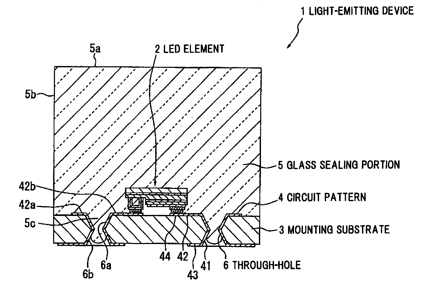
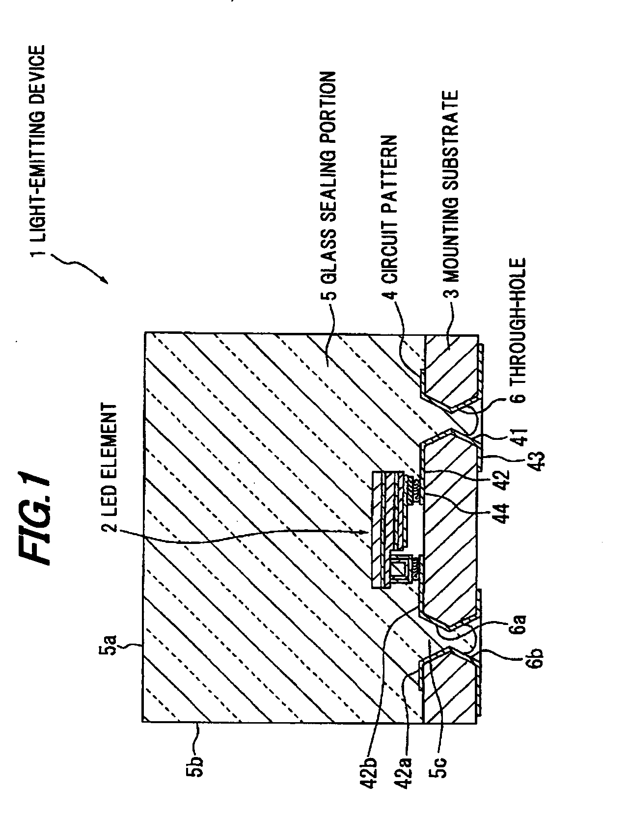
[0056]FIGS. 1 to 8 show an embodiment of the invention and FIG. 1 is a schematic vertical cross sectional view showing a light-emitting device. It should be noted that the size of each portion is different from the actual size in each of the drawings in order to clearly show the configuration of each portion.

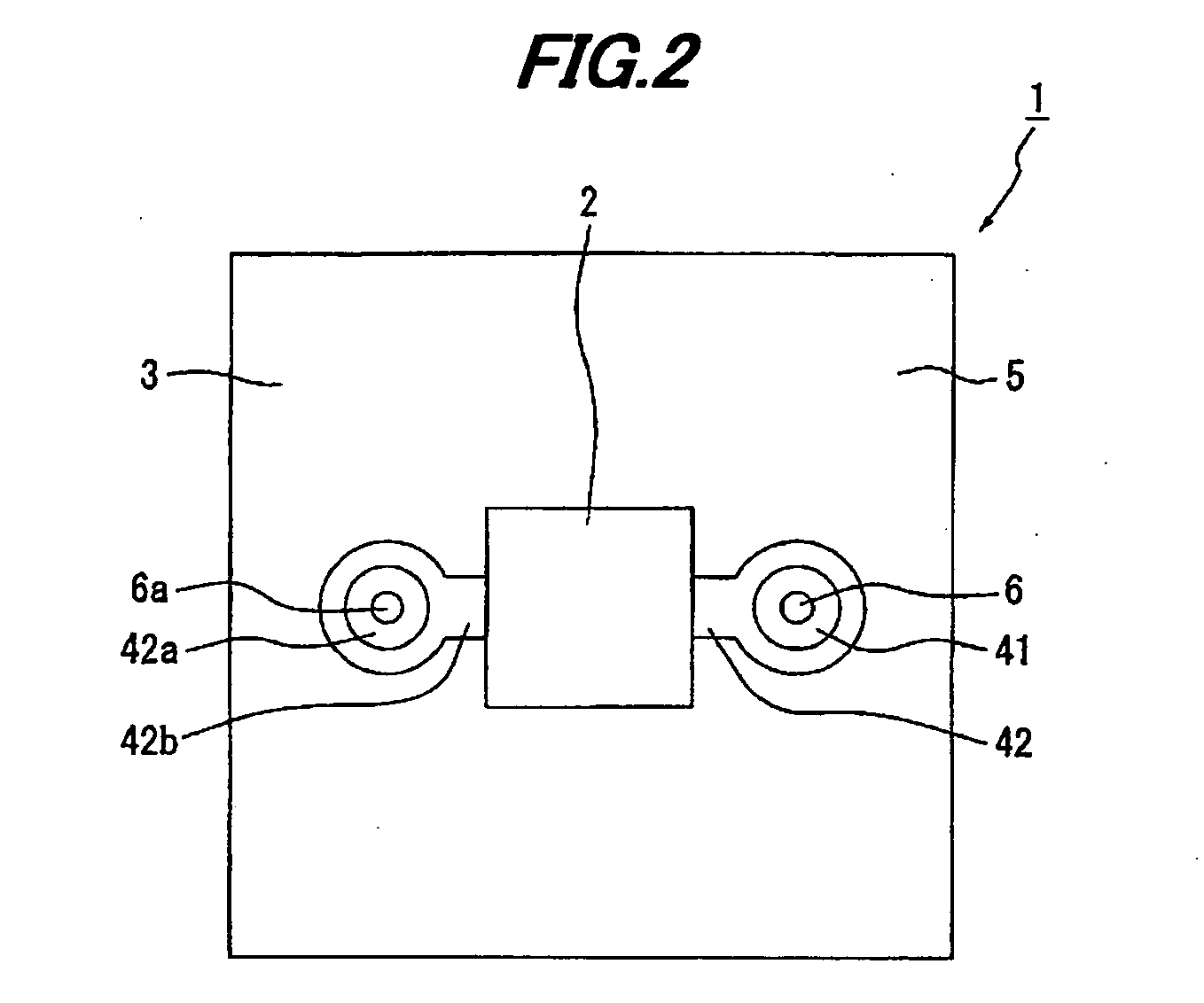
[0057]As shown in FIG. 1, a light-emitting device 1 has a flip-chip-type LED element 2 formed of a GaN-based semiconductor material, a mounting substrate 3 for mounting the LED element 2, a circuit pattern 4 formed on the mounting substrate 3, and a glass sealing portion 5 as an inorganic sealing portion which seals the LED element 2 and is adhered to the mounting substrate 3. In addition, a hollow portion, to where glass does not enter, is formed between the LED element 2 and the mounting substrate 3.

[0058]A through-hole 6 continuing from a front surface to a back surface is formed in the mounting substrate 3. In the present embodiment, the through-hole 6 is each formed on an a...


PUM


Abstract

A method of manufacturing a light-emitting device includes a hole forming process for forming a through-hole that continues from a front surface to a back surface of a mounting substrate, a pattern forming process for continuously forming a circuit pattern on an inner surface of the through-hole in the mounting substrate, from an end portion of the through-hole on the front surface of the mounting substrate to a mounting portion of a light-emitting element, and on a periphery of the through-hole on the back surface of the mounting substrate, a mounting process for mounting the light-emitting element on the mounting portion, and a hot pressing process in that an inorganic material softened by heating is placed on the surface of the mounting substrate and is advanced into the through-hole while sealing the light-emitting element by pressing and bonding the inorganic material to the surface of the mounting substrate.

Description

[0001]The present application is based on Japanese Patent Application No. 2010-062514 filed on Mar. 18, 2010, the entire contents of which are incorporated herein by reference.BACKGROUND OF THE INVENTION [0002]1. Field of the Invention[0003]The invention relates to a light-emitting device that a light-emitting element is mounted on the surface of a mounting substrate and sealed with an inorganic material, a method of manufacturing the same, a method of mounting the same and a lighting device equipped with the same.[0004]2. Description of the Related Art[0005]Conventionally, a method of manufacturing an electronic component is known in which multiple electronic component elements are placed on an insulating substrate, an assembly of the bonded electronic component elements are collectively sealed with resin and is subsequently separated into individual electronic components by dicing (see JP-A 2000-200927). This method includes an insulating substrate manufacturing process for manufa...

Claims


Application Information

Patent Timeline
Patent Type & Authority Applications(United States)
IPC IPC(8): H01L33/56H01L21/603
CPCH01L25/0753H01L33/486H01L33/54H01L33/56H01L2933/005H01L2924/01322H01L24/97H01L2224/16225H01L2924/00H01L2924/15747H01L2924/15787H01L2924/181
Inventor SUEHIRO, YOSHINOBUYAMAGUCHI, SEIJIARAKANE, KATSUNORITASUMI, KOJI
Owner TOYODA GOSEI CO LTD
Why Eureka
Try Eureka