Semiconductor device and method of fabricating the same

a semiconductor memory and semiconductor technology, applied in the field of semiconductor memory devices, can solve the problems of very limited integration degree of two-dimensional semiconductor memory devices

Active Publication Date: 2011-05-26
SAMSUNG ELECTRONICS CO LTD
View PDF7 Cites 102 Cited by
  • Summary
  • Abstract
  • Description
  • Claims
  • Application Information

AI Technical Summary

Problems solved by technology

However, since the highest-priced equipments may be necessary for forming hyper-fine patterns, the integration degree of the two-dimensional semiconductor memory devices is very limited.

Method used


Image

  • Semiconductor device and method of fabricating the same
  • Semiconductor device and method of fabricating the same
  • Semiconductor device and method of fabricating the same

Examples


first exemplary embodiment

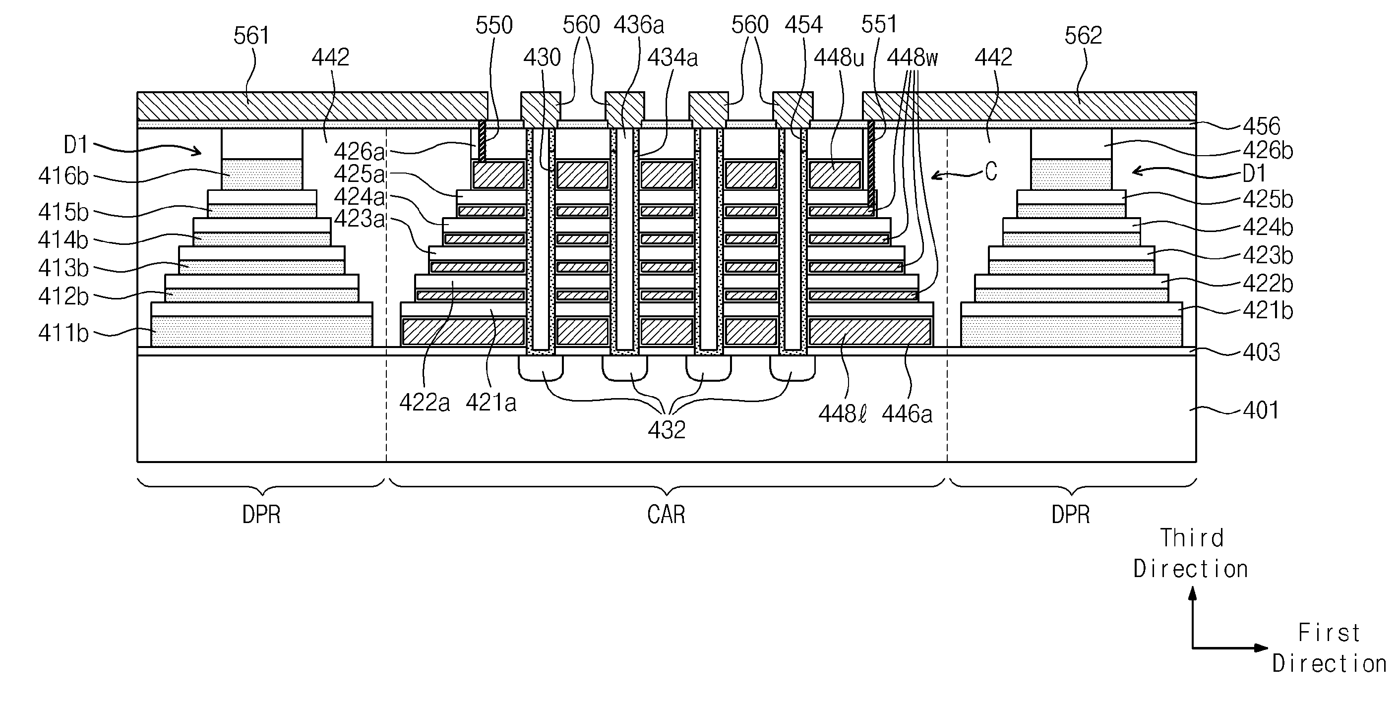
[0051]FIG. 3 illustrates a detailed plane view of a semiconductor device according to a first exemplary embodiment. FIGS. 4A and 4B illustrate cross-sectional views taken along the lines I-I′ and II-II′ of FIG. 3, respectively.

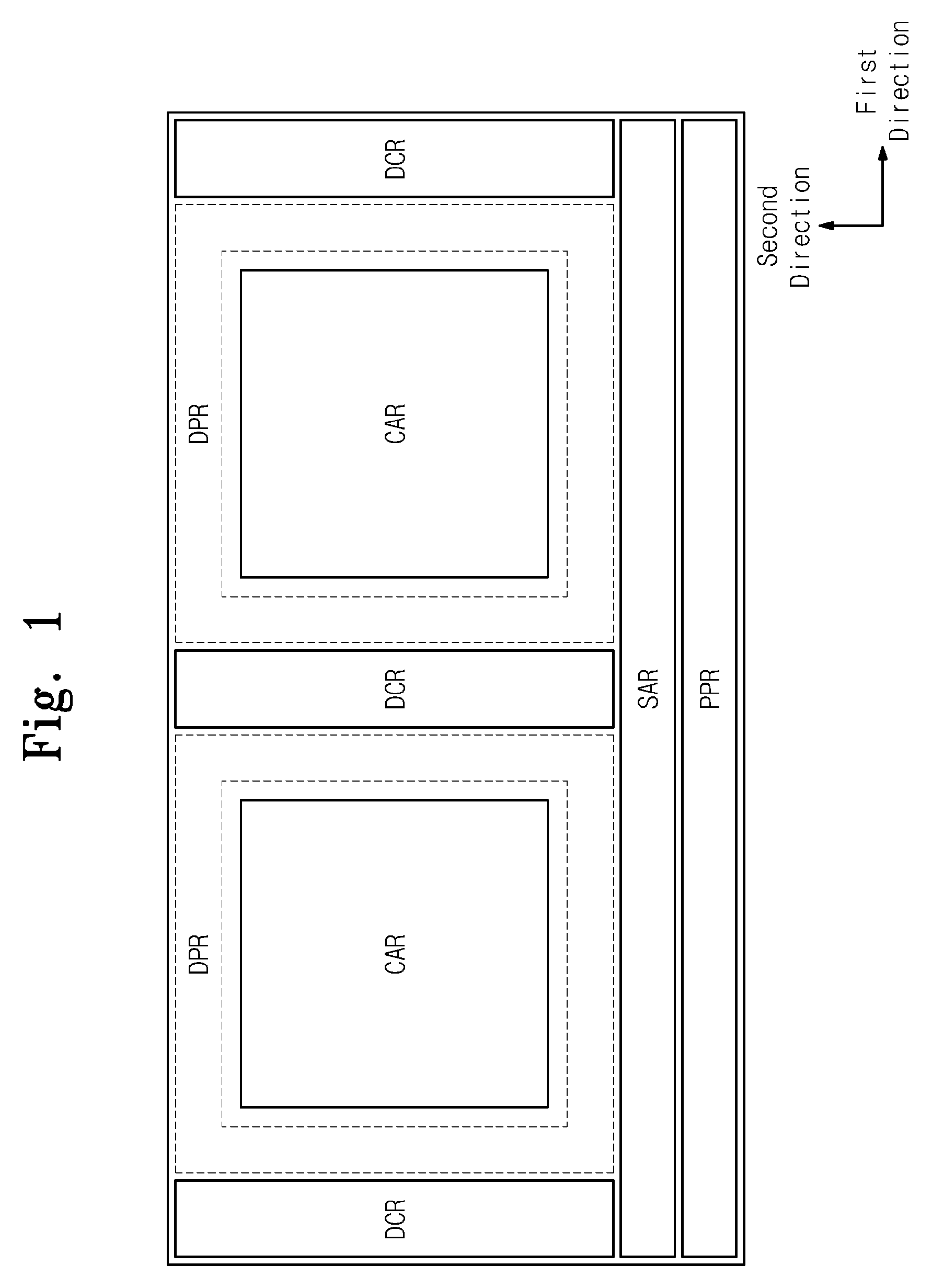
[0052]Referring to FIGS. 3, 4A, and 4B, the semiconductor device according to the first exemplary embodiment includes a semiconductor substrate 401 having the cell array region CAR and the dummy pattern surrounding the cell array region CAR. For example, a P-type impurity layer may be formed on the semiconductor substrate 401. A well region may be formed in the semiconductor substrate 401 (not shown). Substantially the entire surface of the semiconductor substrate 401 may be covered with a buffer layer 403. The buffer layer 403 may include at least one of a silicon oxide layer, a silicon nitride layer, and an oxynitride layer. The buffer layer 403 may protect the semiconductor substrate 401 and may act as an etching protective layer. A cell structure C may be ...

second exemplary embodiment

[0075]FIG. 13 is a detailed plane view of a semiconductor device according to a second exemplary embodiment. FIGS. 14A and 14B are cross-sectional views taken along the lines I-I′ and II-II′ of FIG. 13, respectively.

[0076]In the semiconductor device according to the second exemplary embodiment, referring to FIGS. 13, 14A, and 14B, a damp-proof structure D2 may include a damp-proof reinforcement structure 470 penetrating the dummy sacrificial patterns 411b to 416b and the dummy interlayer insulating patterns 421b to 426b, which are alternately stacked. An upper surface of the damp-proof reinforcement structure 470 may come in contact with the damp-proof layer 456. The damp-proof reinforcement structure 470 may include, e.g., a silicon nitride layer. The damp-proof reinforcement structure 470 may be disposed so as to surround the cell structure C.

[0077]It is possible to form the damp-proof reinforcement structure 470 by forming a third groove (not illustrated) in the dummy pattern reg...

third exemplary embodiment

[0079]FIG. 15 is a detailed plane view of a semiconductor device according to a third exemplary embodiment. FIGS. 16A and 16B are cross-sectional views taken along the lines I-I′ and II-II′ of FIG. 15, respectively.

[0080]In the semiconductor device according to the third exemplary embodiment, referring to FIGS. 15, 16A, and 16B, a damp-proof structure D3 may include the damp-proof reinforcement structure 470 penetrating the dummy sacrificial patterns 411b to 416b and the dummy interlayer insulating patterns 421b to 426b, which are alternately stacked. Furthermore, the damp-proof structure D3 may include a dummy active pattern 434b interposed between the damp-proof reinforcement structure 470 and the dummy sacrificial patterns 411b to 416b and between the damp-proof reinforcement structure 470 and the dummy interlayer insulating patterns 421b to 426b. An upper surface of the damp-proof reinforcement structure 470 may be lower than that of the dummy active pattern 434b. A protective i...


PUM


Abstract

A semiconductor device has a substrate that includes a cell array region and a dummy pattern region surrounding the cell array region. The cell array region includes a cell structure having a plurality of cell active pillars extending in a vertical direction from the cell array region of the substrate and includes cell gate patterns and cell gate interlayer insulating patterns alternately stacked on the substrate. The cell gate patterns and cell gate interlayer insulating patterns have sides facing the cell active pillars. The dummy pattern region includes a damp-proof structure.

Description

CROSS-REFERENCE TO RELATED APPLICATIONS[0001]This application is a continuation-in-part of U.S. patent application Ser. No. 12 / 588,270, filed Oct. 9, 2009, entitled “Vertical-type semiconductor device and method of manufacturing the same.”BACKGROUND[0002]1. Field[0003]Embodiments relate to a semiconductor device and a method of fabricating the same, and to a vertical-type nonvolatile memory device and a method of fabricating the same.[0004]2. Description of the Related Art[0005]In response to users' needs, good performance and low price may be sought for semiconductor devices. To address the users' needs, semiconductor devices may have an increased integration degree. For example, in semiconductor memory devices, the integration degree may be a significant factor for determining prices. In particular, in two-dimensional or planar semiconductor memory devices, the integration degree may be determined by an occupying area of each unit memory cell. The memory devices are also greatly i...

Claims


Application Information

Patent Timeline
Patent Type & Authority Applications(United States)
IPC IPC(8): H01L27/088
CPCH01L27/11526H01L27/11529H01L27/11551H01L27/11556H01L27/11573H01L21/36H01L29/66825H01L29/66833H01L29/7881H01L29/792H01L29/7926H01L27/11578H01L21/02521H10B41/40H10B41/41H10B41/20H10B43/40H10B43/20H10B41/27
Inventor LEE, SEUNG-JUNLEE, WOONKYUNG
Owner SAMSUNG ELECTRONICS CO LTD
Why Eureka
Try Eureka