Two-wire dimmer switch for low-power loads

Active Publication Date: 2011-05-26
LUTRON TECH CO LLC
View PDF51 Cites 167 Cited by
  • Summary
  • Abstract
  • Description
  • Claims
  • Application Information

AI Technical Summary

Benefits of technology

[0017]According to an embodiment of the present invention, a two-wire load control device (such as, a dimmer switch) is able to control the amount of power delivered from an AC power source to an electrical load (such as, a high-efficiency lighting load) and has substantially no minimum load requirement. The dimmer switch includes a bidirectional semiconductor switch that is adapted to be coupled in series electrical connection between the AC power source and

Problems solved by technology

However, prior art reverse phase-control dimmer switches have either required neutral connections and/or advanced control circuits (such as microprocessors) for controlling the operation of the FETs.
These advanced control circuits and power supplies add to the cost of prior art FET-based reverse phase-control dimmer switches (as compared to analog forward phase-control dimmer switches).
If the power rating of the lighting load is too low, the charging current conducted by the power supply through the lighting load may be great enough to cause the lighting load to illuminate to a level that is perceptible to the human eye when the lighting load is off.
High-efficiency light sources typically consume less power and provide longer operational lives as compared to incandescent and halogen lamps.
However, the load regulation devices for the high-efficiency light sources may have high input impedances or input impedances that vary in magnitude throughout a half-cycle.
Therefore, when a prior-art forward phase-control dimmer switch is coupled between the AC power source and the load regulation device for the high-efficiency light source, the load control

Method used


Image

  • Two-wire dimmer switch for low-power loads
  • Two-wire dimmer switch for low-power loads
  • Two-wire dimmer switch for low-power loads

Examples


first embodiment

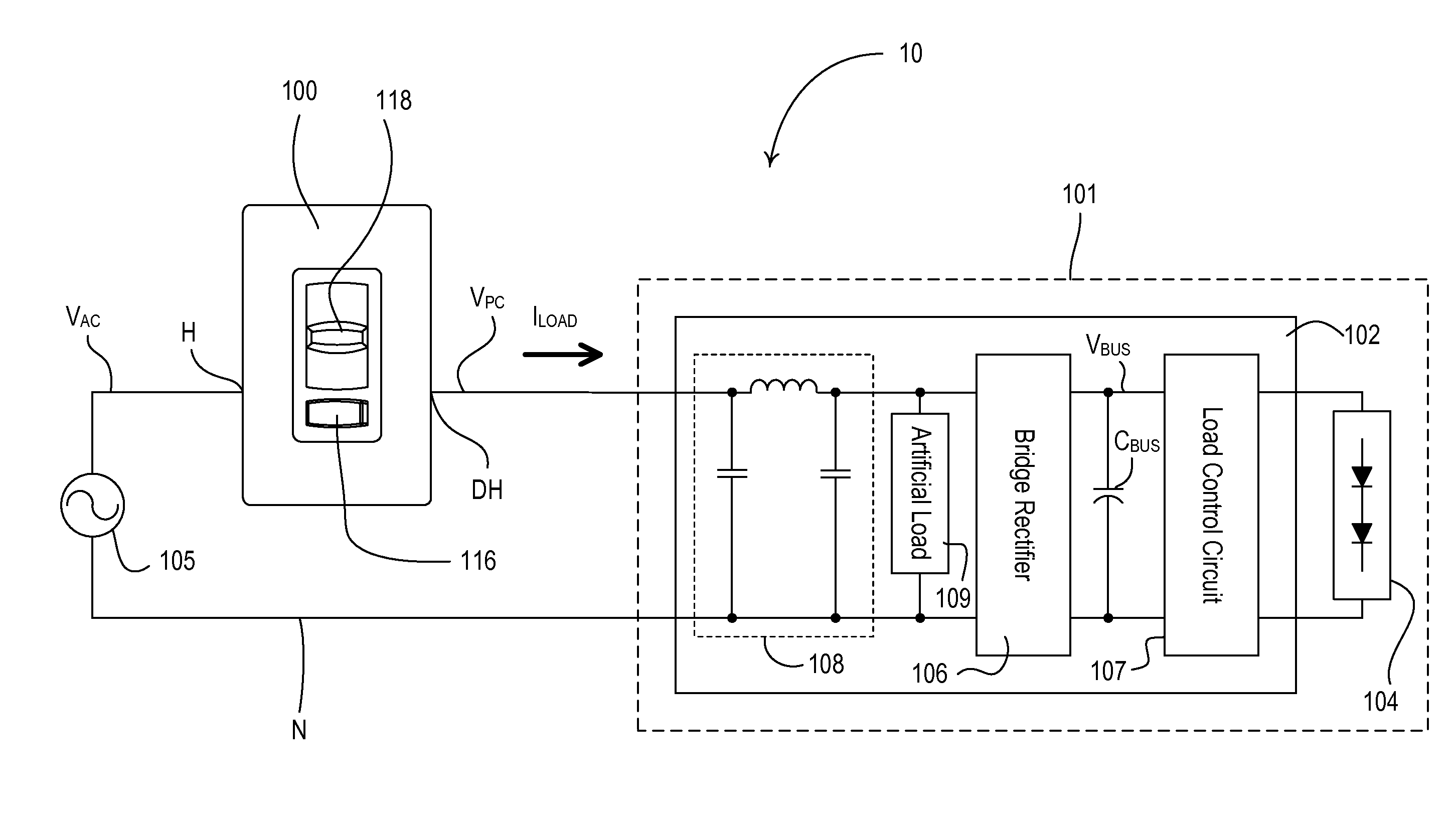
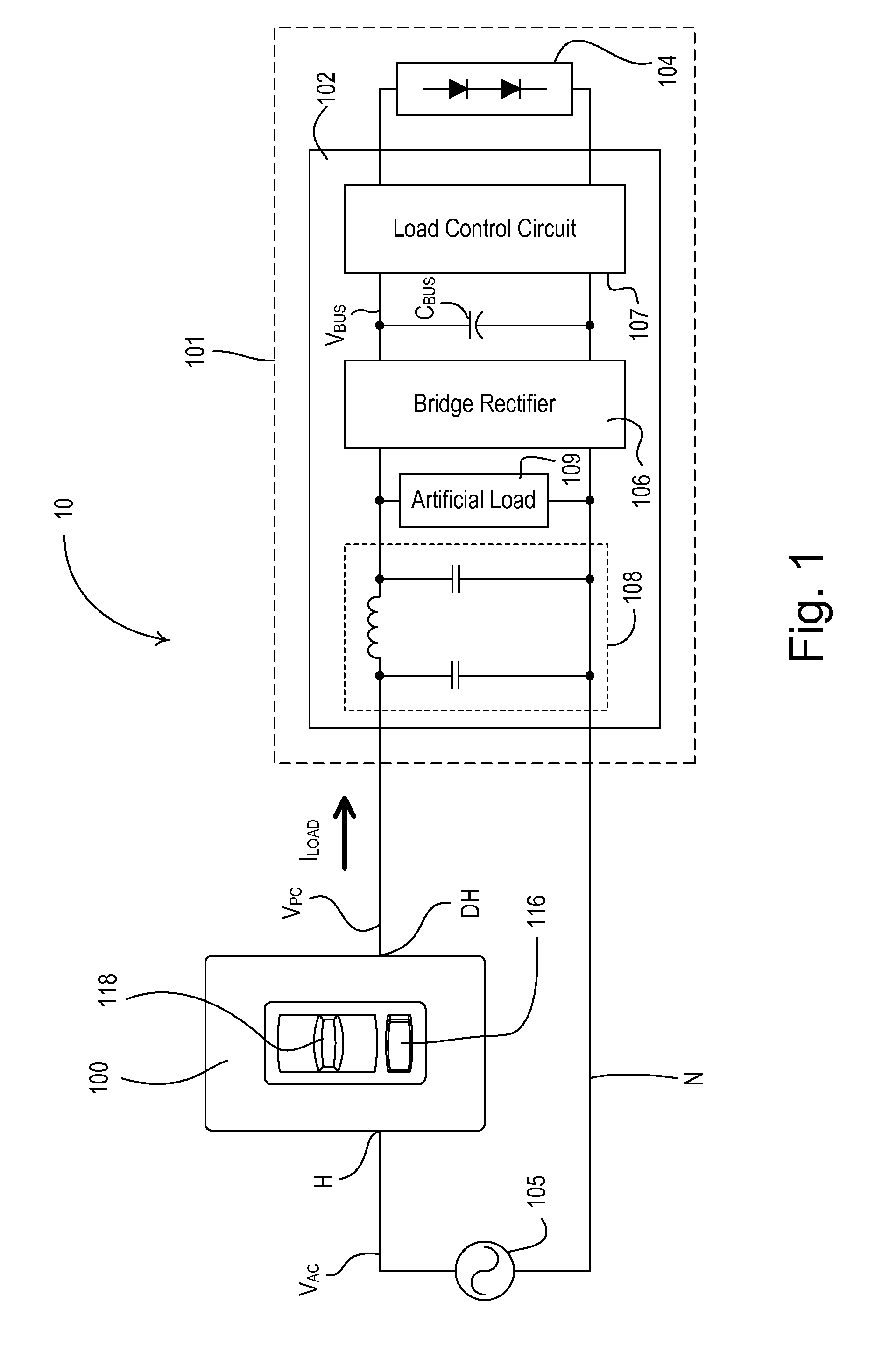
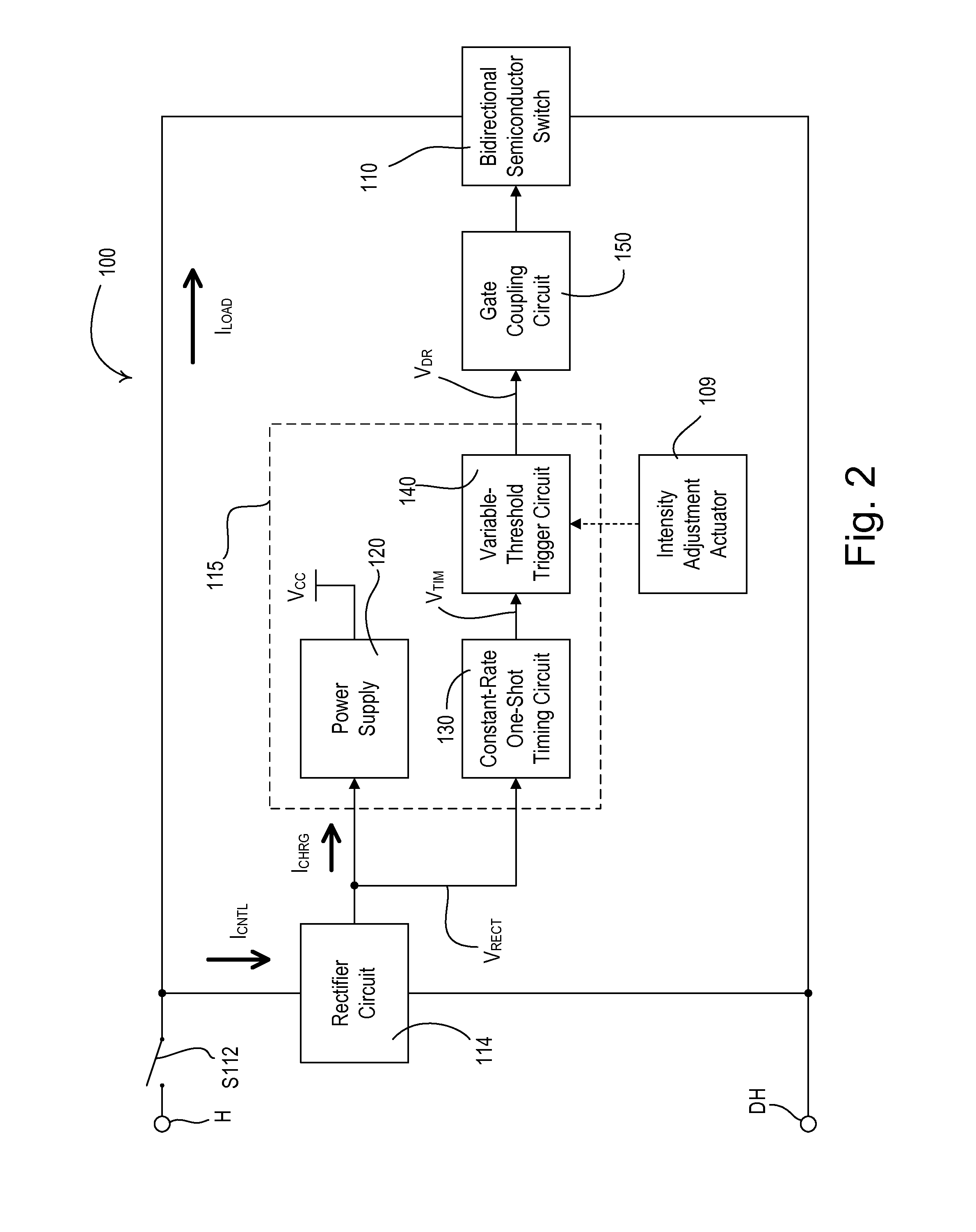
[0056] the dimmer switch 100 comprises an analog control circuit 115 including a power supply 120, a constant-rate one-shot timing circuit 130, and a variable-threshold trigger circuit 140 (i.e., a gate drive circuit). The control circuit 115 receives the rectified voltage VRECT from the rectifier circuit 114 and conducts a control current ICNTL through the load (i.e., the LED driver 102) in order to generate a drive voltage VAR for controlling the bidirectional semiconductor switch 110 to thus adjust the intensity of the LED light source 104 in response to the intensity adjustment actuator 118. The power supply 120 of the control circuit 115 conducts a charging current ICHRG through the LED driver 102 in order to generate a supply voltage VCC (e.g., approximately 11.4 volts). The charging current ICHRG of the power supply makes up a portion of the control current ICNTL of the control circuit 115.

[0057]The timing circuit 130 receives the supply voltage VCC and generates a timing vol...

third embodiment

[0081]FIG. 8 is a simplified timing diagram showing examples of the phase-control voltage VPC generated by the dimmer switch 300, the timing voltage VTIM, and the gate voltage VG for driving the FETs Q210A, Q210B according to the present invention. The phase-control voltage VPC has a magnitude equal to approximately the magnitude of the AC line voltage VAC of the AC power source 105 at the beginning of each half-cycle during a conduction time TCON, and has a magnitude of approximately zero volts during the rest of the half-cycle, i.e., during a non-conduction time TNC. To generate the phase-control voltage VPC, the gate drive circuit 340 drives the gate voltage VG high towards the reference voltage VREF at the beginning of each half-cycle, such that the FETs Q210A, Q210B are rendered conductive (as shown at time t1 in FIG. 8). At this time, the timing circuit 330 begins generating the timing voltage VTIM, which comprises a ramp voltage that increases in magnitude with respect to tim...

fifth embodiment

[0092]FIG. 12 is a simplified timing diagram showing examples of the phase-control voltage VPC generated by the dimmer switch 500 and the gate voltages VG1, VG2 for driving the FETs Q510A, Q510B, respectively. According to the present invention, the phase-control voltage VPC comprises a forward phase-control voltage. During the positive half-cycles, the first FET Q510A is rendered conductive and the second FET Q510B is rendered non-conductive when the first gate voltage VG1 increases from approximately zero volts to the nominal gate voltage VN (as shown at time t1), and the second gate voltage VG2 decreases from the nominal gate voltage VN to approximately zero volts. At this time, the dimmer switch 500 conducts the load current ILOAD to the LED driver 102 through the first FET Q510A and the body diode of the second FET Q510B. At the beginning of the negative half-cycles, the first FET Q510 remains conductive. However, since the second FET Q510B is non-conductive and the body diode ...


PUM


Abstract

A two-wire load control device (such as, a dimmer switch) is operable to control the amount of power delivered from an AC power source to an electrical load (such as, a high-efficiency lighting load) and has substantially no minimum load requirement. The dimmer switch includes a bidirectional semiconductor switch, which is operable to be rendered conductive each half-cycle and to remain conductive independent of the magnitude of a load current conducted through semiconductor switch. The dimmer switch comprises a control circuit that conducts a control current through the load in order to generate a gate drive signal for rendering the bidirectional semiconductor switch conductive and non-conductive each half-cycle. The control circuit may provide a constant gate drive to the bidirectional semiconductor switch after the bidirectional semiconductor switch is rendered conductive each half-cycle. The bidirectional semiconductor switch may comprise, for example, a triac or two field-effect transistors coupled in anti-series connection.

Description

[0001]This application is related to commonly-assigned U.S. Provisional Patent Application No. 61 / 264,528, filed Nov. 25, 2009, and U.S. Provisional Patent Application No. 61 / 333,050, filed May 10, 2010, both entitled TWO-WIRE ANALOG DIMMER SWITCH FOR LOW-POWER LOADS, the entire disclosures of which are hereby incorporated by reference.BACKGROUND OF THE INVENTION[0002]1. Field of the Invention[0003]The present invention relates to load control devices for controlling the amount of power delivered to an electrical load, and more particularly, to a two-wire analog dimmer switch for controlling the intensity of a low-power lighting load, such as a light-emitting diode (LED) light source having an LED driver circuit or a fluorescent lamp having an electronic dimming ballast.[0004]2. Description of the Related Art[0005]Prior art two-wire dimmer switches are coupled in series electrical connection between an alternating-current (AC) power source and a lighting load for controlling the amo...

Claims


Application Information

Patent Timeline
IPC IPC(8): H05B37/02H05B44/00
CPCH05B39/04H05B39/048Y02B20/148H05B33/0845H05B37/02H02M7/06H05B33/0815G05F3/08Y02B20/00H05B47/10H05B45/10
Inventor NEWMAN, JR., ROBERT C.SALVESTRINI, CHRISTOPHER JAMES
Owner LUTRON TECH CO LLC
Why Eureka
Try Eureka