Driving Circuit and Output Buffer

a driving circuit and output buffer technology, applied in the direction of instruments, computing, electric digital data processing, etc., can solve the problems of abnormal display, voltage of the positive and the negative output buffers may not match with each other, etc., to avoid abnormal display and improve display effect

Inactive Publication Date: 2011-05-26
RAYDIUM SEMICON
View PDF5 Cites 2 Cited by
  • Summary
  • Abstract
  • Description
  • Claims
  • Application Information

AI Technical Summary

Benefits of technology

[0006]The invention is directed to an output buffer used for driving first and second output channels, wherein the output buffer includes first and second input stages. The output buffer directed to by the invention switches the transmission path of the input and the output signals of the first and the second input stages with a switch circuit, so that the signals generated and amplified by the first and the second input stages are constantly used as the output signals of the first and the second output channels respectively. In other words, the output buffer directed to by the invention can drive the fixed output channels with fixed input stages. In comparison to the conventional output buffer, the output buffer directed to by the invention effectively avoids the mismatching between the positive and the negative analog driving voltages outputted by the conventional source driver, which occurs due to the mismatching between the threshold voltages of the buffers, hence avoiding the occurrence of abnormal display. Thus, the outputted positive and negative analog driving voltages match with each other and the display effect is improved.

Problems solved by technology

However, the threshold voltages of the positive and the negative output buffers may not match with each other due to process factors.
When mismatching of the threshold voltages occurs, the positive and the negative analog driving voltages outputted by the conventional source driver will not match with each other either, and the occurrence of abnormal display will occur.

Method used


Image

  • Driving Circuit and Output Buffer
  • Driving Circuit and Output Buffer
  • Driving Circuit and Output Buffer

Examples


Embodiment Construction

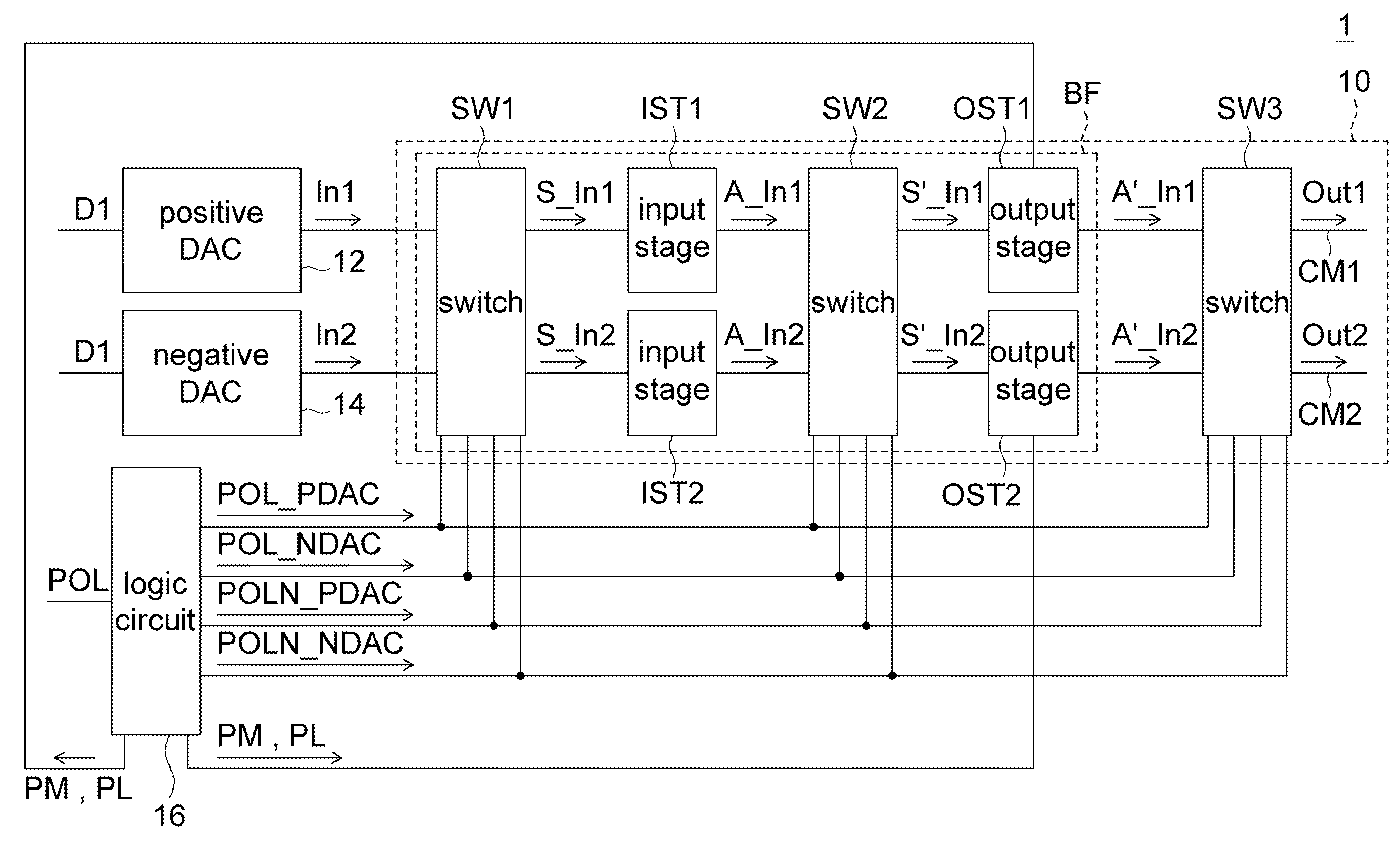
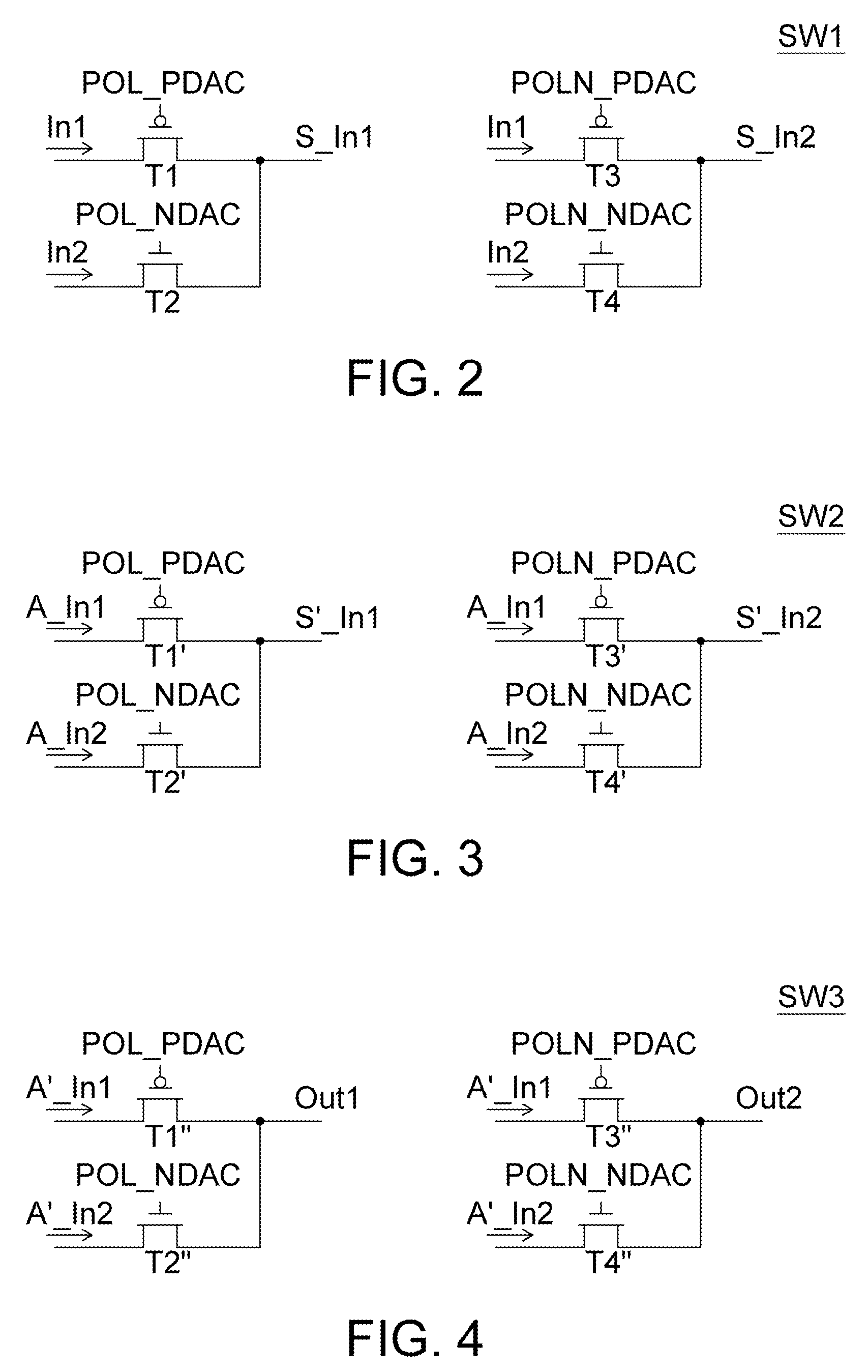
[0017]The driver of an embodiment of the invention switches the transmission path of the input and the output signals of the first and the second input stages with a switch circuit, so that the signals generated and amplified by the first and the second input stages are constantly used as the output signals of the first and the second output channels respectively.

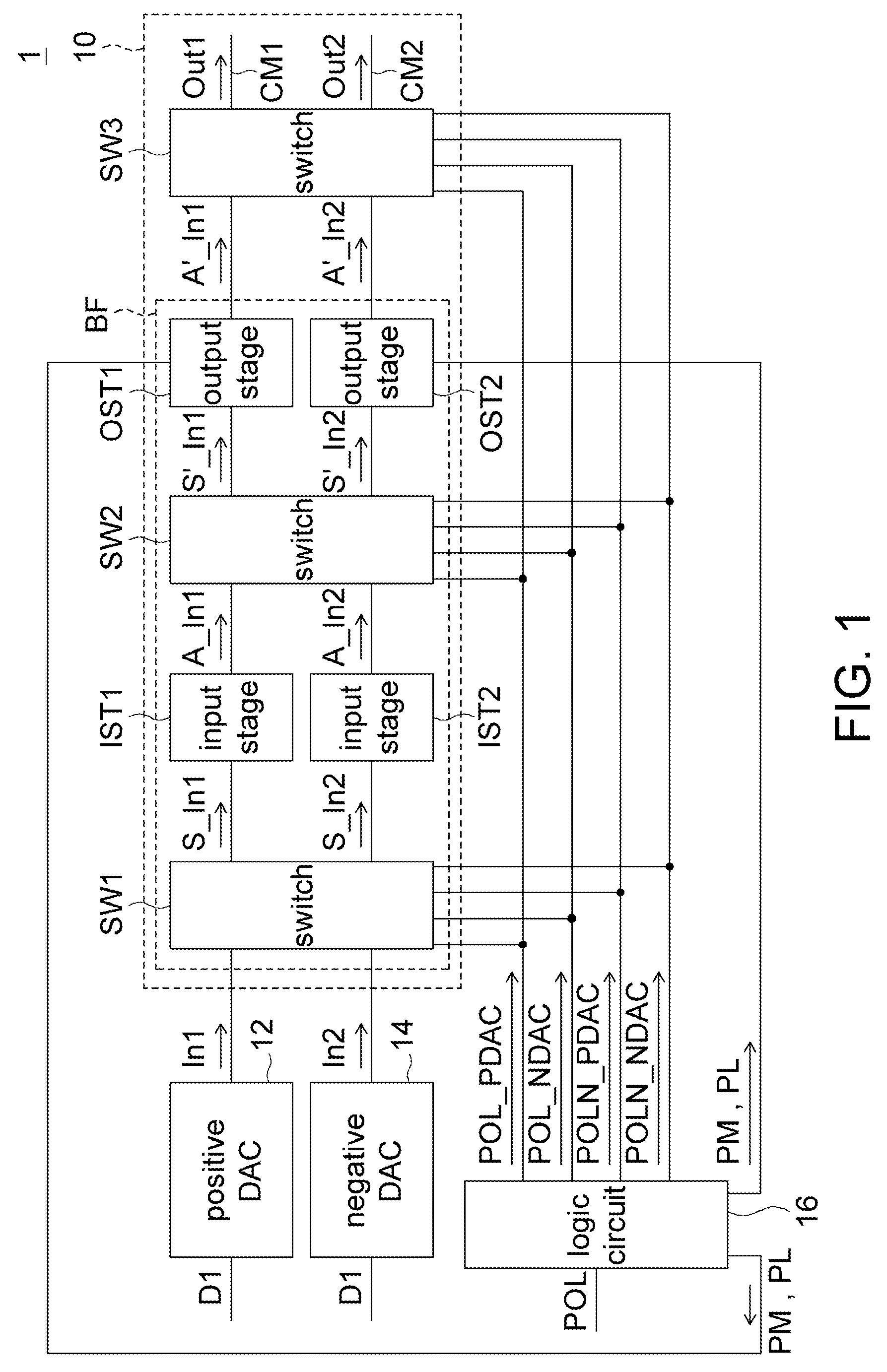
[0018]Referring to FIG. 1, a block diagram of a driver according to an embodiment of the invention is shown. The driver 1 is used in electronic display device such as LCD. In an implementation, the driver 1 is realized by a source driver having a number of output channels for driving a number of pixel columns of the LCD. Only a partial structure of the source driver is illustrated in FIG. 1.

[0019]The driver 1 includes an output buffer 10, and first and second conversion circuits. The first and the second conversion circuits, such as digital analog converter (DAC), respectively provide analog input signals In1 and In2 in res...


PUM


Abstract

An output buffer including a first switch circuit and a buffer is provided. The first switch circuit receives first and second input signals. The buffer circuit includes first and second input stages, first and second output stages and a second switch circuit. The first and the second input stages are coupled to the first switch circuit. The first and the second output stages are coupled to the second switch circuit. The second switch circuit, coupled to the first and the second input stages and the first and the second output stages, selectively couples one of first and the second input stages to the first output stage and selectively couples the other to the second output stage. The first switch circuit further selectively provides one of the first and the second input signals to the first input stage and selectively provides the other to the second input stage.

Description

[0001]This application claims the benefit of Taiwan application Serial No. 098140419, filed Nov. 26, 2009, the subject matter of which is incorporated herein by reference.BACKGROUND OF THE INVENTION[0002]1. Field of the Invention[0003]The invention relates in general to a driver, and more particularly to a driver used in electronic display device.[0004]2. Description of the Related Art[0005]Liquid crystal display (LCD) having the advantages of low radiation and low power consumption, has become the mainstream display product. The LCD normally includes a number of source drivers, which provides an analog driving voltage to drive the LCD panel. Conventionally, a source driver would employ two sets of output buffers to provide positive and negative output voltages. Thus, in response to each output channel, the source driver can, in different frame periods, provide analog driving voltages with a non-inverted polarity or that with an inverted polarity to the LCD panel. However, the thres...

Claims


Application Information

Patent Timeline
Patent Type & Authority Applications(United States)
IPC IPC(8): G06F3/038
CPCG09G3/3614G09G2310/0291G09G2310/027G09G3/3685
Inventor TSO, KO-YANGMIAO, HUI-WENLO, YU-LUNGLIANG, YANN-HSIUNGWU, HSIN-YEH
Owner RAYDIUM SEMICON
Why Eureka
Try Eureka