Image forming apparatus, image forming method, and process cartridge

a technology of image forming and process cartridge, which is applied in the direction of electrographic process, corona discharge, instruments, etc., can solve the problems of high exchange rate, high cost, and high cost of photoconductors, so as to prevent abnormal images, stable forming high-resolution images, and high abrasion resistance

Inactive Publication Date: 2012-12-18
RICOH KK
View PDF45 Cites 1 Cited by
  • Summary
  • Abstract
  • Description
  • Claims
  • Application Information

AI Technical Summary

Benefits of technology

[0018]The present invention aims to solve the various conventional problems and achieve the following objects. Namely, the present invention aims to provide an image forming apparatus, an image forming method, a process cartridge each of which allows for stably forming high-resolution images over a long period of time while preventing occurrences of abnormal images that would be caused by repetitive use in high-speed operation by using a latent electrostatic image bearing member having a surface layer and a photosensitive layer each having high-abrasion resistance, high-durability and excellent electric properties.
[0019]As a result of keen examinations provided by the present inventors in view of the above noted problems to solve the conventional problems, the present inventors could find the following. Namely, the present inventors found that it is possible to obtain an image forming apparatus which is highly durable and allows for stably forming high-resolution images over a long period of time while preventing occurrences of abnormal images attributable to residual negative images that would be formed on a latent electrostatic image bearing member by the effect of transfer bias generated from a transferring unit when the latent electrostatic image bearing member is repeatedly charged and exposed in high-speed operation in the image forming apparatus; the image forming apparatus allows for high-speed operation and employing a method of which a visible image formed on the latent electrostatic image bearing member is transferred onto a recording medium by applying a positive electric potential to a visible image formed on the latent electrostatic image bearing member; the latent electrostatic image bearing member has a photosensitive layer and a surface layer, the surface layer contains a hardened material composed of a trifunctional or more radical polymerizable compound having no charge transporting structure, a radical polymerizable compound having a charge transporting structure, and a reactive silicone compound, and the concentration of the reactive silicone compound is varied in between the surface part of the surface layer and the innerlayer part of the surface layer to thereby obtain the above-noted latent electrostatic image bearing member. Further, the present inventors found that by setting the concentration of the reactive silicone compound at the innerlayer part of the surface layer to be higher than the concentration thereof at the surface part of the surface layer, occurrences of abnormal images can be significantly prevented even when the surface layer is gradually worn away. These findings led to the completion of the present invention.

Problems solved by technology

Further, recently, demands for full-color laser printers and full-color digital copiers allowing for printing full-color images have become bulged rapidly.
With advancement in technologies of making photoconductors have smaller diameters, photoconductors cannot avoid being used under harsher environments.
Therefore, with conventional photoconductors, the exchange rate thereof is drastically increased, and a further serious problem may be caused particularly in high-speed machines.
As the result, hazard applied to corresponding regions the toner developed on a photoconductor and other regions of the photoconductor significantly influences image-formation even via a recording medium, thereby causing abnormal images.
With respect to the former, a fatigue of a photoconductor is worse due to repetitive charging and exposing of the photoconductor at the time of forming an image, and reductions in electric potential of charge caused by the fatigue or increases in electric potential caused by the fatigue result in degradation of quality of images.
In particular, a reduction in electric potential of charge further increases influence of the leaked charge from the conductive substrate to cause background smear.
With respect to the latter, the surface layer of the photoconductor is worn away due to friction with a cleaning member or the like, and then the film thickness of the photoconductor surface layer is reduced, consequently, degradation of quality of images is caused due to an increased charge intensity and increased scratches on the photoconductor surface, and the like.
However, among these photoconductors, (i) the photoconductor using a curable binder is insufficient in solubility with charge transporting materials, and thus a residual charge potential tends to be increased due to effect of impurities such as polymerization initiator and unreacted residues to thereby cause degradation in image density.
Further, (ii) the photoconductor using a polymer charge transporting material makes it possible to improve abrasion resistance thereof to some extent, however, the photoconductor has not yet attained the level to satisfactorily satisfy durability required for organic photoconductors.
In addition, since it is difficult to polymerize and refine a polymer charge transporting material and it is hard to obtain a highly pure polymer charge transporting material, the electric properties are rarely stabilized in the material.
Further, a problem in production may be caused, for example, a coating solution using a polymer charge transporting material has high viscosity.
(iii) the photoconductor in which an organic filler is dispersed in a crosslinked charge transporting layer can exert high-abrasion resistance as compared to a typical photoconductor in which a low-molecular weight charge transporting material is dispersed in an inactive polymer, however, residual electric potential tends to be easily increased due to charge traps residing on the inorganic filler surface to thereby cause degradation in image density.
When the degree of convexoconcave or irregularity induced to the inorganic filler and a binder resin of the photoconductor surface is great, cleaning defects may occur to cause toner filming and image deletion.
Thus, with the use of the photoconductors of (i), (ii), and (iii), there are still problems with residual electric potential and surface cleaning property, which may cause image defects, and the proposed photoconductors have not yet attained the level to satisfy the required durability.
In addition, when a low-molecular weight charge transporting material was simply contained in a crosslinked charge transporting layer, there was a difficulty with solubility with the hardened material, and insufficient solubility with the hardened material actually causes precipitation of the low-molecular weight charge transporting material and white turbidity phenomenon to cause increases in electric potential in exposed regions.
The increases in electric potential result in not only a degraded image density but also a degraded mechanical strength.
Specifically, in the photoconductor, a monomer is reacted in a condition where a polymer binder is contained, and therefore, a three-dimensional (3D) network is not sufficiently formed and the crosslink density is sparse, and thus the photoconductor has not yet attained the level of exerting remarkable abrasion resistance.
The photoconductor allows for achieving both abrasion resistance and excellent electric properties and draws attention, however, when a binder resin having no reactivity is used, the solubility between the binder resin and a hardened material prepared by reacting the monomer with the charge transporting material is poor, layer separation occurs in the crosslinked charge transporting layer, which may cause scratches of the photoconductor surface, and adhesion of external additives and paper powder in a toner.
As described above, a three-dimensional (3D) network is not sufficiently formed and the crosslink density is sparse, and accordingly the photoconductor has not yet attained the level of exerting remarkable abrasion resistance.
Even when a binder resin having reactivity is used, although the molecular mass of the hardened material is increased, the number of crosslinked molecules is also small, it is difficult to achieve both sufficient bonding amount and sufficient crosslink density of the charge transporting material, and it cannot be said that the photoconductor meets a satisfactory level of electric property and abrasion resistance.
The cause is not yet clearly revealed, and the reason is assumed that the crosslinked film is deteriorated by some factors.
As the result, the charge potential is reduced at the sites, and a residual negative image is generated after exposure of the photoconductor surface to thereby develop an abnormal image.
When the inside of the surface layer is exposed outside, the inside of the crosslinked film has already been deteriorated, and residual negative images increasingly occur.

Method used


Image

  • Image forming apparatus, image forming method, and process cartridge
  • Image forming apparatus, image forming method, and process cartridge
  • Image forming apparatus, image forming method, and process cartridge

Examples


examples

Synthesis Example of Monofunctional Compound Having a Charge Transporting Structure

[0370]The monofunctional compound having a charge transporting structure of the present invention can be synthesized by a method described in Japanese Patent (JP-B) No. 3164426. On example of the synthesis method will be described below.

(1) Synthesis of Hydroxy Group-Substituted Triarylamine Compound (Represented by the Following Structural Formula B)

[0371]In a vessel, 240 mL of sulfolane was added to 113.85 g (0.3 mol) of a methoxy group-substituted triarylamine compound (represented by the following Structural Formula A) and 138 g (0.92 mol) of sodium iodide, and the mixture solution was heated to 60° C. in a nitrogen stream. Into the mixture solution, 99 g (0.91 mol) of trimethylchlorosilane was delivered by drops for 1 hour, and the mixture solution was stirred at a temperature of about 60° C. for 4.5 hours, and then the reaction was stopped. To the reaction solution, about 1.5 L of toluene was ad...

synthesis example i-1

—Synthesis of Titanyl Phthalocyanine Pigment—

[0379]In a vessel, 292 g of 1,3-diiminoisoindoline was mixed with 2,000 mL of sulfolane, and 204 g of titanium tetrabuthoxide was delivered by drops into the mixture solution under a nitrogen stream. Upon completion of the dripping, the temperature of the mixture solution was gradually raised to 180° C., and the mixture solution was stirred for 5 hours while keeping the reaction temperature ranging from 170° C. to 180° C. to perform a reaction. After completion of the reaction, the reaction solution was left to cool, and then the obtained precipitate was filtered, and the filtered precipitate was washed with chloroform until the powder turned into blue color.

[0380]Next, the filtered precipitate was washed with methanol several times, further washed with hot water of 80° C. several times, and then dried to thereby obtain a coarse titanyl phthalocyanine.

[0381]The obtained titanyl phthalocyanine was dissolved in 20 times its volume of a conc...

production example i-1

—Preparation of Latent Electrostatic Image Bearing Member—

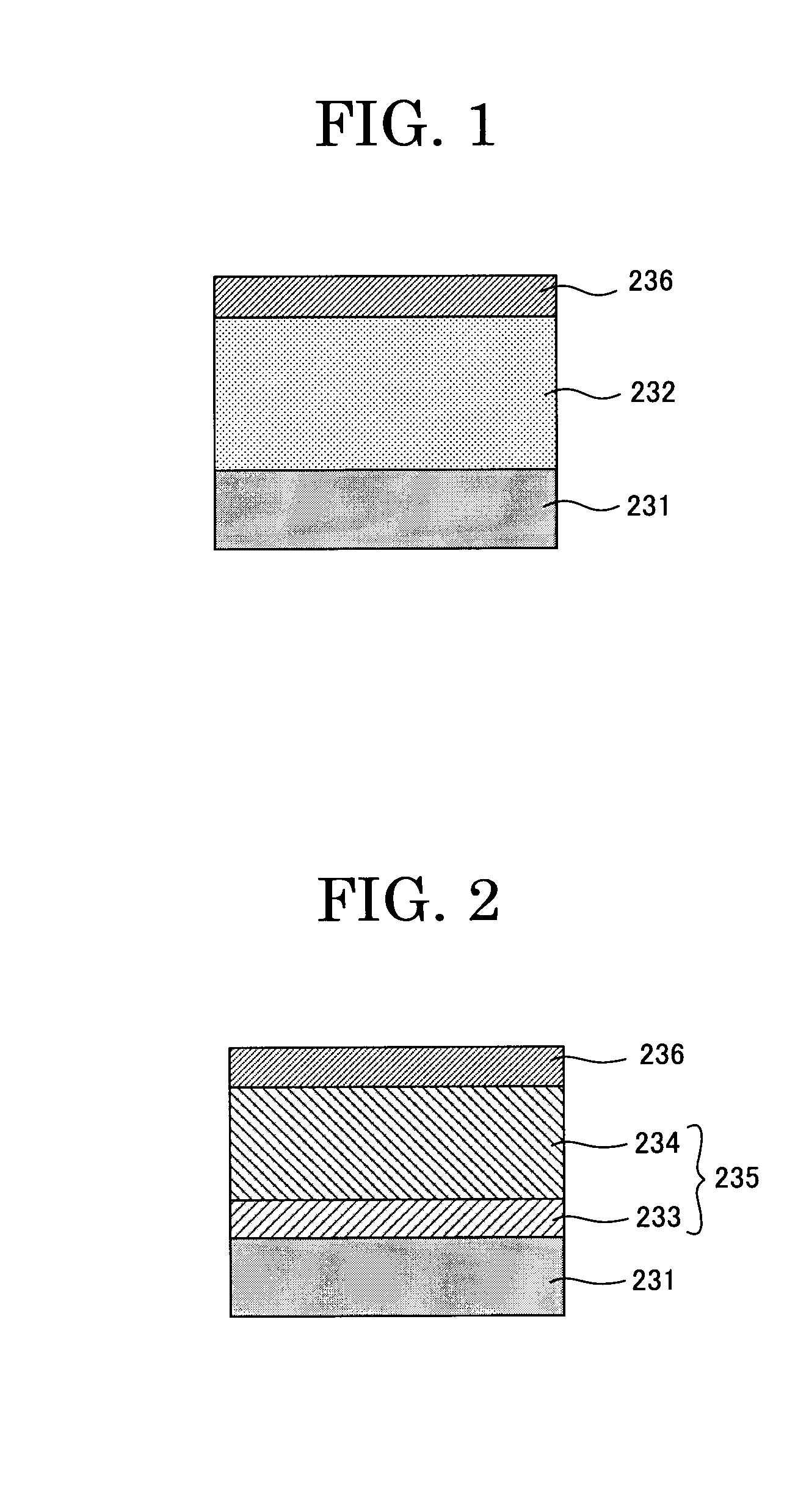
[0391]Over the surface of an aluminum cylinder having a diameter of 100 mm, an undercoat layer coating solution containing the following composition, a charge generating layer coating solution containing the following composition, and a charge transporting layer coating solution containing the following composition were sequentially applied and dried to thereby form an undercoat layer having a thickness of 3.5 μm, a charge generating layer having a thickness of 0.3 μm, and a charge transporting layer having a thickness of 23 μm on the cylinder.

[0392]Over the surface of the obtained charge transporting layer, a surface layer coating solution A and a surface layer coating solution B each containing the following composition were sequentially applied by spray-coating and then the cylinder surface with the surface layer coating solution A and the surface layer coating solution B applied thereon was irradiated with a light beam un...


PUM

PropertyMeasurementUnit
Bragg angle 2θaaaaaaaaaa
angleaaaaaaaaaa
angleaaaaaaaaaa

Abstract

The present invention provides an image forming apparatus which is equipped with at least a latent electrostatic image forming unit, a developing unit, a transferring unit, and a fixing unit, wherein the transferring unit is configured to apply a positive electric potential to a visible image formed on the latent electrostatic image bearing member via a recording medium, the latent electrostatic image member has a surface layer which comprises a hardened material hardened by irradiating at least a trifunctional or more radical polymerizable compound having no charge transporting structure, a radical polymerizable compound having a charge transporting structure, and a reactive silicone compound having any one of an acryloyloxy group and a methacryloyloxy group, and the concentration of the reactive silicone compound is varied in between the surface part and the innerlayer part of the surface layer.

Description

BACKGROUND OF THE INVENTION[0001]1. Field of the Invention[0002]The present invention relates to an image forming apparatus, an image forming method, and a process cartridge each of which allows for stably forming high-resolution images over a long period of time while preventing occurrences of abnormal images that would be caused by repetitive use in high-speed operation by using a latent electrostatic image bearing member (may be hereinafter referred to as “photoconductor” and “electrophotographic photoconductor”) which has a surface layer and a photosensitive layer each having high-abrasion resistance, high-durability and excellent electric properties.[0003]2. Description of the Related Art[0004]In recent years, technologies of information processing system machines using an electrophotographic method have been remarkably advanced. In particular, performance of laser printers and digital copiers of which information is converted into digital signals to record the information by m...

Claims


Application Information

Patent Timeline
Patent Type & Authority Patents(United States)
IPC IPC(8): G03G15/00
CPCG03G5/0542G03G5/0546G03G5/0578G03G5/0589G03G5/0592G03G5/0614G03G5/14795G03G5/14734G03G5/14739G03G5/14773G03G5/14786G03G5/14791G03G5/071G03G15/00G03G5/072G03G5/0732G03G5/074G03G5/0745
Inventor KAWASAKI, YOSHIAKIYANAGAWA, YOSHIKIHIROSE, MITSUAKI
Owner RICOH KK
Why Eureka
Try Eureka