Pattern Transfer Modeling for Optical Lithographic Processes
a technology of optical lithography and pattern density distribution, applied in the field of integrated circuit design and manufacturing, can solve the problems of reducing the feature size correspondingly, increasing the difficulty of faithfully reproducing the image intended by the layout design onto the substrate, and not taking into account the pattern density distribution of layout segments in the conventional optimization process, so as to achieve the effect of etching transfer, the effect of unaccounted for pattern densities
- Summary
- Abstract
- Description
- Claims
- Application Information
AI Technical Summary
Benefits of technology
Problems solved by technology
Method used
Image

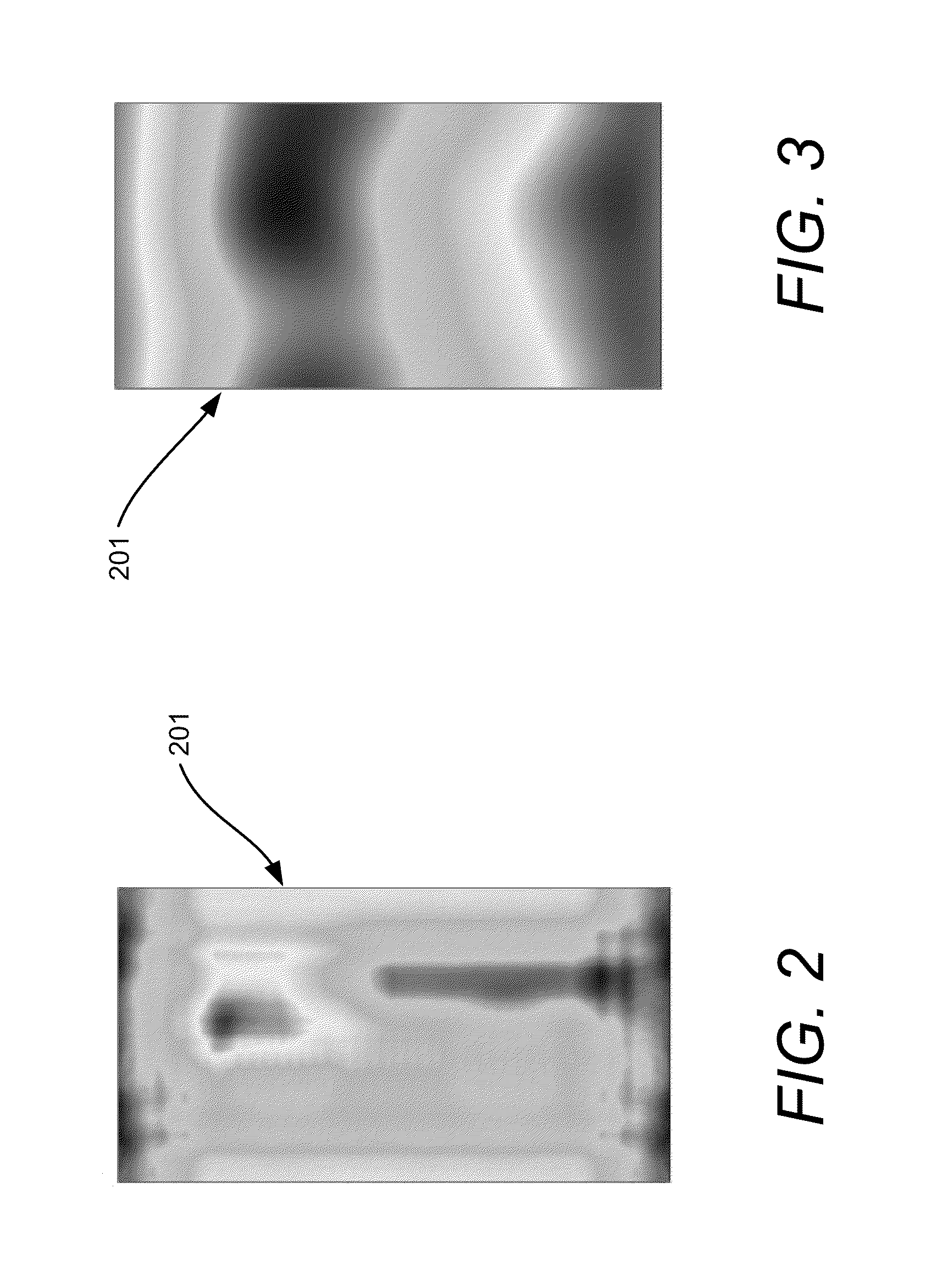
Examples
Embodiment Construction
[0028]The operations of the disclosed implementations may be described herein in a particular sequential order. However, it should be understood that this manner of description encompasses rearrangements, unless a particular ordering is required by specific language set forth below. For example, operations described sequentially may in some cases be rearranged or performed concurrently. Moreover, for the sake of simplicity, the illustrated flow charts and block diagrams typically do not show the various ways in which particular methods can be used in conjunction with other methods.
[0029]It should also be noted that the detailed description sometimes uses terms like “determine” to describe the disclosed methods. Such terms are often high-level abstractions of the actual operations that are performed. The actual operations that correspond to these terms will often vary depending on the particular implementation, and will be readily discernible by one of ordinary skill in the art.
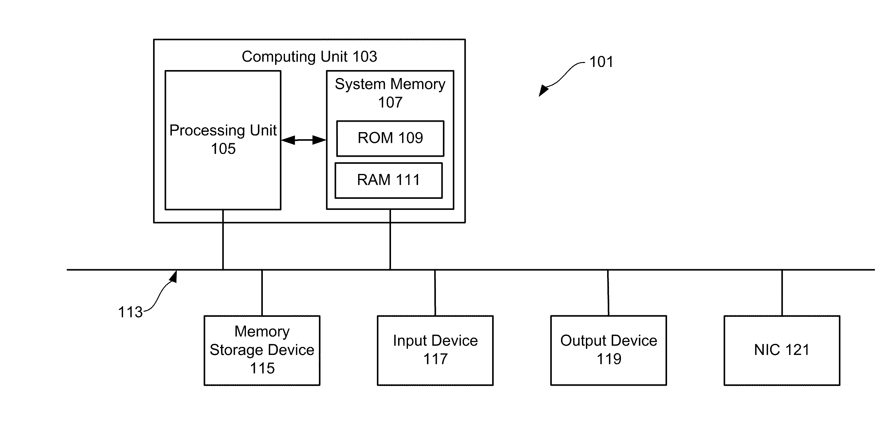
[0030...
PUM
 Abstract
Description
Claims
Application Information