Enhancement normally off nitride semiconductor device and method of manufacturing the same

a semiconductor device and normally off technology, applied in the field of nitride semiconductor devices, can solve the problems of low efficiency, fluctuation of source-drain current, complicated and expensive driving circuits of normally on devices, etc., and achieve the effect of simple driving circuit and easy implementation

Active Publication Date: 2011-06-16
KYUNGPOOK NAT UNIV IND ACADEMIC COOP FOUND
View PDF5 Cites 20 Cited by
  • Summary
  • Abstract
  • Description
  • Claims
  • Application Information

AI Technical Summary

Benefits of technology

[0016]In this manner, the present invention provides a method of easily implementing a normally off enhancement semiconductor device by removing a hetero-junction layer with selective etching or a masking barrier below a gate region, thereby originall

Problems solved by technology

Normally on devices are less preferable for power applications, because (a) these devices are operated with less efficiency than normally off devices and (b) driving circuits for the

Method used


Image

  • Enhancement normally off nitride semiconductor device and method of manufacturing the same
  • Enhancement normally off nitride semiconductor device and method of manufacturing the same
  • Enhancement normally off nitride semiconductor device and method of manufacturing the same

Examples


Embodiment Construction

[0020]Hereinafter, preferred embodiments of the present invention will be described in detail with reference to the accompanying drawings.

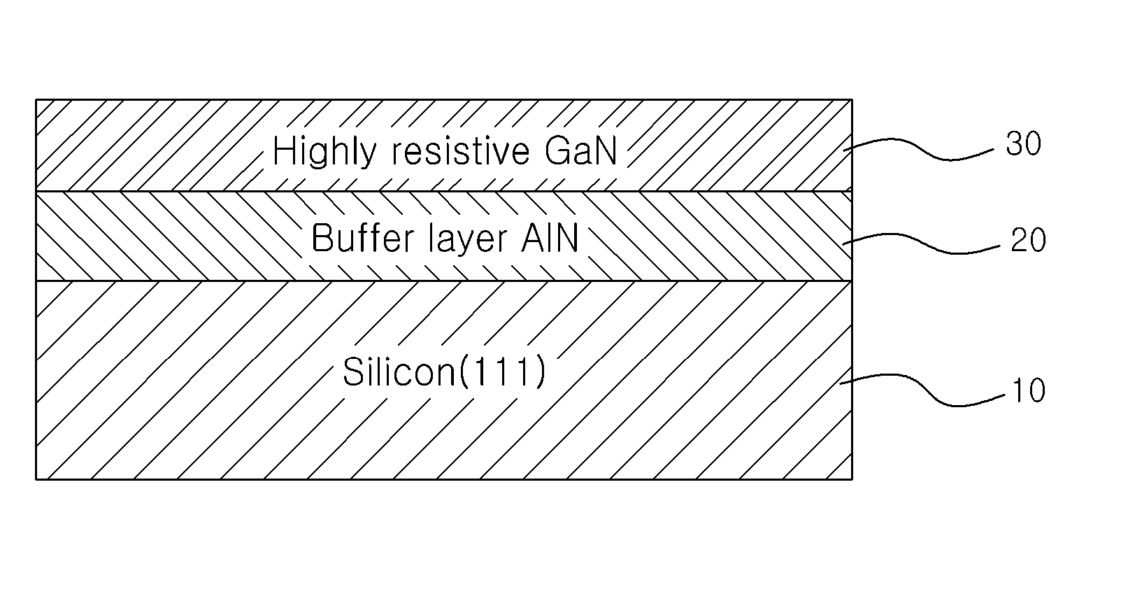
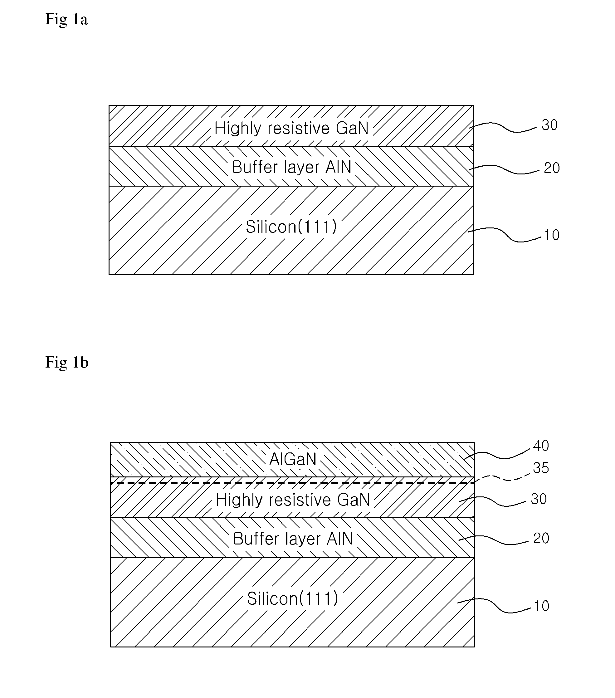
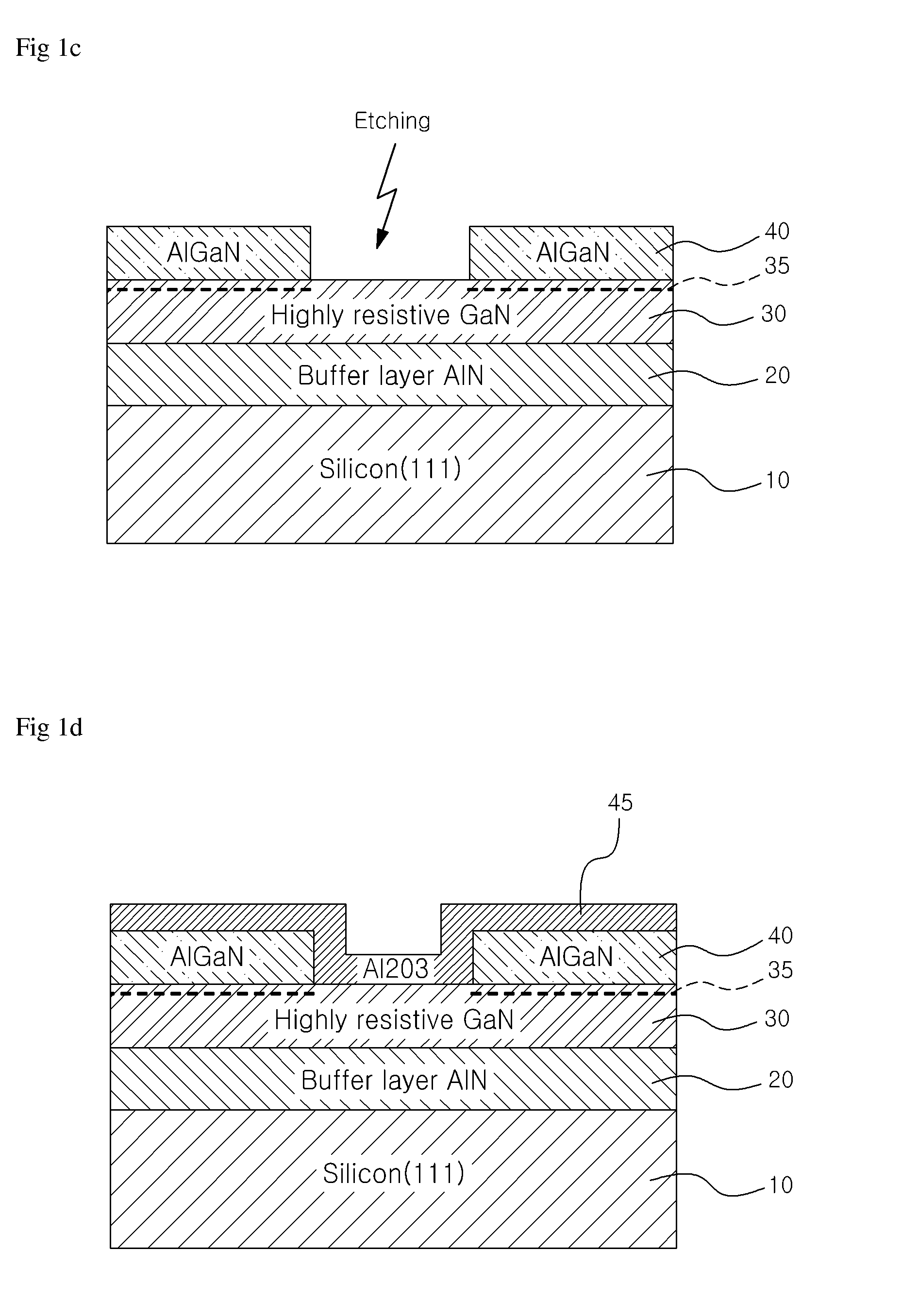
[0021]FIG. 1 (1a to 1e) is a view showing processes of manufacturing a normally off nitride semiconductor device according to an embodiment of the present invention, and FIG. 3 is a flow diagram showing processes of manufacturing the normally off nitride semiconductor device according to an embodiment of the present invention. Hereinafter, preferred embodiments of the present invention will be described in detail with reference to FIGS. 1 and 3.

[0022]A method of manufacturing a normally off nitride semiconductor device according to an embodiment of the present invention generally includes a step (S100) of forming a buffer layer 20 on a substrate 10; a step (S200) of forming a first nitride semiconductor layer 30 on the buffer layer 20; a step (S300) of forming a second nitride semiconductor layer 40 on the first nitride semiconductor layer 30; a s...


PUM


Abstract

The present invention relates to an enhancement normally off nitride semiconductor device and a method of manufacturing the same. The method includes the steps of: forming a buffer layer on a substrate; forming a first nitride semiconductor layer on the buffer layer; forming a second nitride semiconductor layer on the first nitride semiconductor layer; etching a gate region above the second nitride semiconductor layer up to a predetermined depth of the first nitride semiconductor layer; forming an insulating film on the etched region and the second nitride semiconductor layer; patterning a source/drain region, etching the insulating film in the source/drain region, and forming electrodes in the source/drain region; and forming a gate electrode on the insulating film in the gate region. In this manner, the present invention provides a method of easily implementing a normally off enhancement semiconductor device by originally blocking 2DEG which is generated under a gate region. In addition, the present invention provides an enhancement normally off power semiconductor device with a simple and efficient driving circuit in a HEMT device.

Description

TECHNICAL FIELD[0001]The present invention relates to a nitride semiconductor device and a method of manufacturing the same, and more particularly, to an enhancement normally off nitride semiconductor device and a method of manufacturing the device easily using a selective etching and a masking barrier.BACKGROUND ART[0002]HEMT (high electron mobility transistor) is one example of traditional power semiconductor devices. HEMT is manufactured using a III group nitride semiconductor, which means semiconductor alloyed metal from GaN, AlGaN, InGaN or AlInGaN system, as mentioned in this specification.[0003]As known in the traditional art, HEMT includes a first III group nitride semiconductor body composed of, for example, undoped GaN, and a second III group semiconductor body which is arranged on the first III group nitride semiconductor body and is composed of, for example, AlGaN.[0004]As well known in the art, hetero-junction between the first III group nitride semiconductor body and t...

Claims


Application Information

Patent Timeline
IPC IPC(8): H01L29/78H01L21/336
CPCH01L29/1033H01L29/2003H01L29/7787H01L29/66462H01L29/517H01L29/778
Inventor LEE, JUNG HEEIM, KI SIKHA, JONG BONG
Owner KYUNGPOOK NAT UNIV IND ACADEMIC COOP FOUND
Why Eureka
Try Eureka