Organic-light emitting device, light equipment including the same, and organic light-emitting display apparatus including the same
a light-emitting device and light-emitting display technology, applied in the direction of basic electric elements, electrical devices, semiconductor devices, etc., can solve the problems of limiting overall an external quantum efficiency and a power factor, affecting the lifespan of the organic-light-emitting device, etc., to achieve the effect of improving the out-coupling efficiency
- Summary
- Abstract
- Description
- Claims
- Application Information
AI Technical Summary
Benefits of technology
Problems solved by technology
Method used
Image
Examples
first embodiment
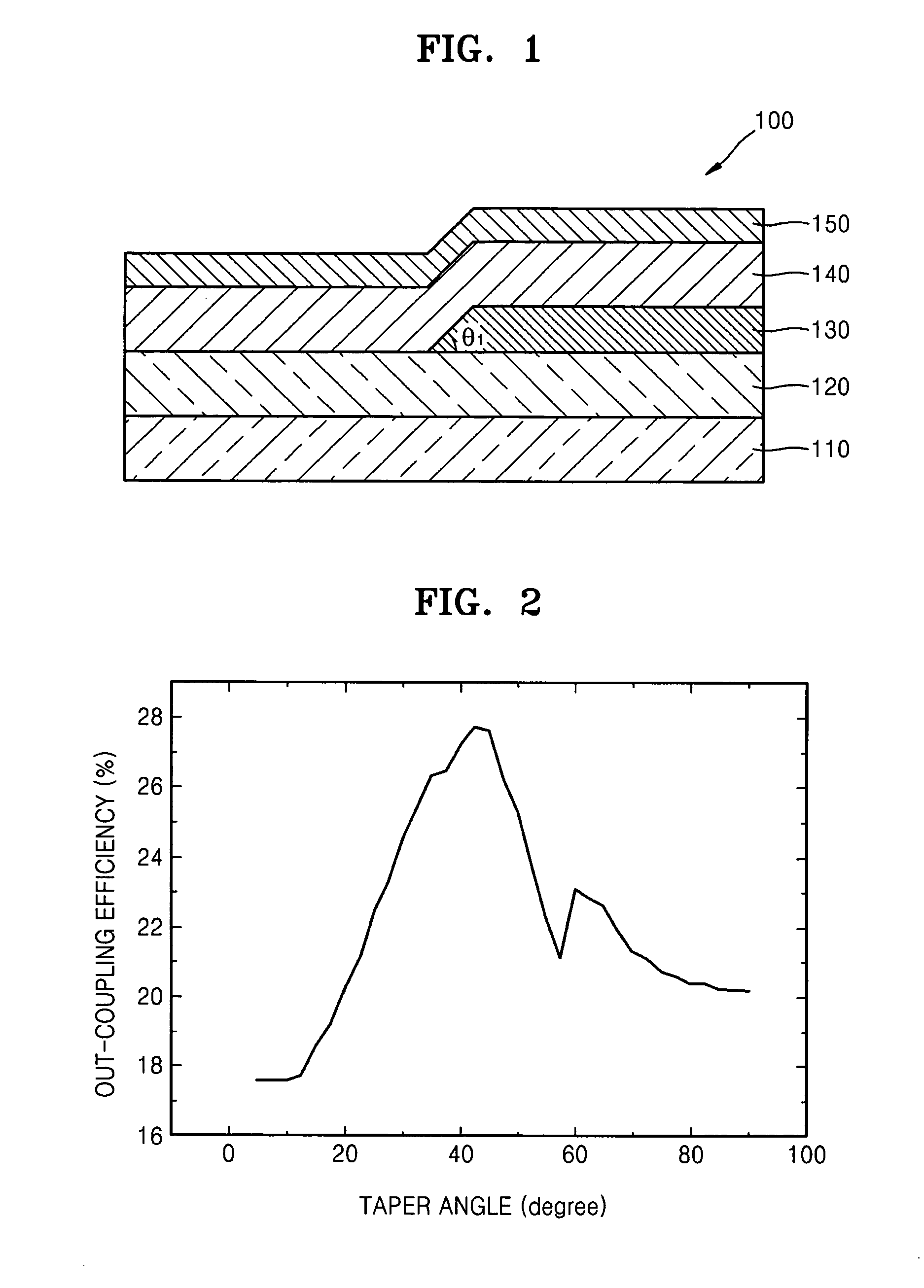
[0047]FIG. 1 illustrates a schematic cross-sectional view of an organic light-emitting device 100 according to a
[0048]In the example embodiment illustrated in FIG. 1, the organic light-emitting device 100 includes a substrate 110, a first electrode layer 120, a low refractive layer 130, an organic light-emitting layer 140, and a second electrode layer 150.
[0049]The substrate 110 may be, e.g., a glass substrate using SiO2 as a main component, a plastic substrate, or a substrate formed of various types of materials. The organic light-emitting device 100 of the present embodiment may be applied to a top-emission organic light-emitting device (for emitting light toward the second electrode layer 150), may be applied to a bottom-emission organic light-emitting device (for emitting light toward the substrate 110), or may be applied to a two-sided emission organic light-emitting device. In the following description, the organic-light emitting device 100 of the present embodiment is a botto...
second embodiment
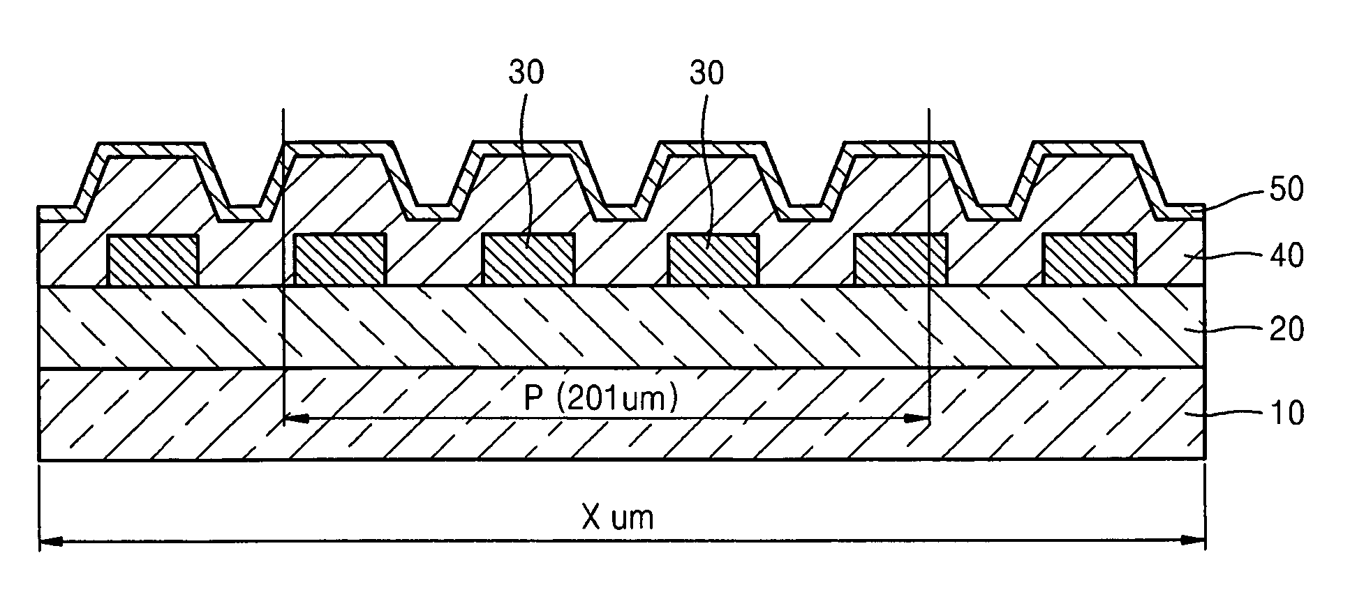
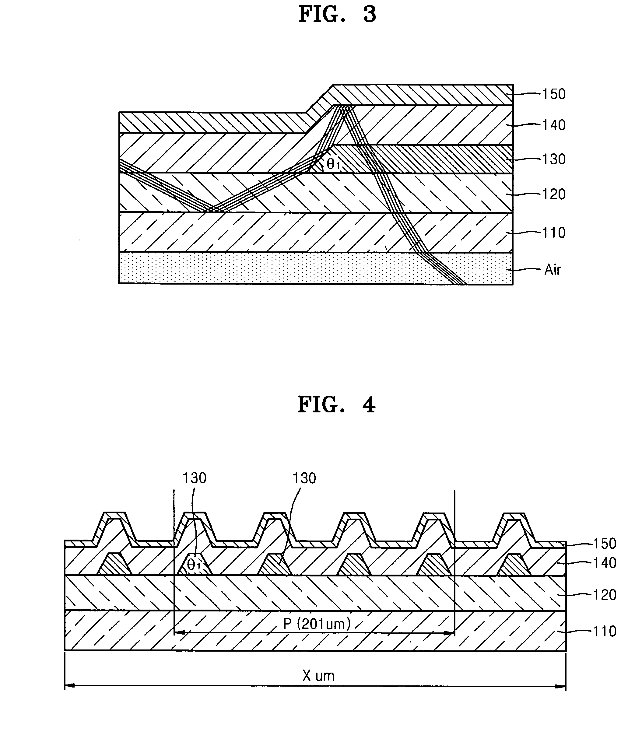
[0063]FIG. 4 illustrates a cross-sectional view of an organic light-emitting device 130 including a low refractive layer formed in a regular pattern at a taper angle of 45° according to a FIG. 5 illustrates a cross-sectional view of a comparative organic light-emitting device including a low refractive layer 30 having a taper angle of 90°.
[0064]Each light emitting part “P” is distributed within a range of 201 μm×201 μm so as to correspond to the size of one pixel. Each of the low refractive layers 130 and 30 is widely distributed in a regular pattern having a size of 3 μm×3 μm within a range between 10,000 μm×1,000 μm in order to check effects on adjacent pixels. Each substrate 110 and 10 is formed to a thickness of 700 μm.
[0065]FIG. 6 illustrates a graph of normalized power values of the OLED of FIG. 4 and the OLED of FIG. 5 according to a size of a photoreceiver. FIG. 7 illustrates a graph of first-order derivatives of the normalized power values of FIG. 6;
[0066]Referring to FIG....
fifth embodiment
[0081]FIG. 12 illustrates a schematic cross-sectional view of an organic light-emitting device 200 according to a
[0082]In the example embodiment shown in FIG. 12, the organic light-emitting device 200 includes a substrate 210, a first electrode layer 220, a high refractive layer 230, an organic light-emitting layer 240, and a second electrode layer 250.
[0083]The organic light-emitting device 200 includes the high refractive layer 230 instead of the low refractive layer 130 of the organic light-emitting device 100 of the first embodiment, and characteristics relating to this difference will be described in detail below.
[0084]The organic light-emitting device 200 may be applied to a top-emission organic light emitting device (which emits light toward the second electrode layer 250), may be applied to a bottom-emission organic light emitting device (which emits light toward the substrate 210), or may be applied to a two-sided light emitting device. The organic light-emitting device 200...
PUM
 Abstract
Description
Claims
Application Information


