

Method of controlling etch microloading for a tungsten-containing layer
- Summary
- Abstract
- Description
- Claims
- Application Information
AI Technical Summary
Benefits of technology
Problems solved by technology
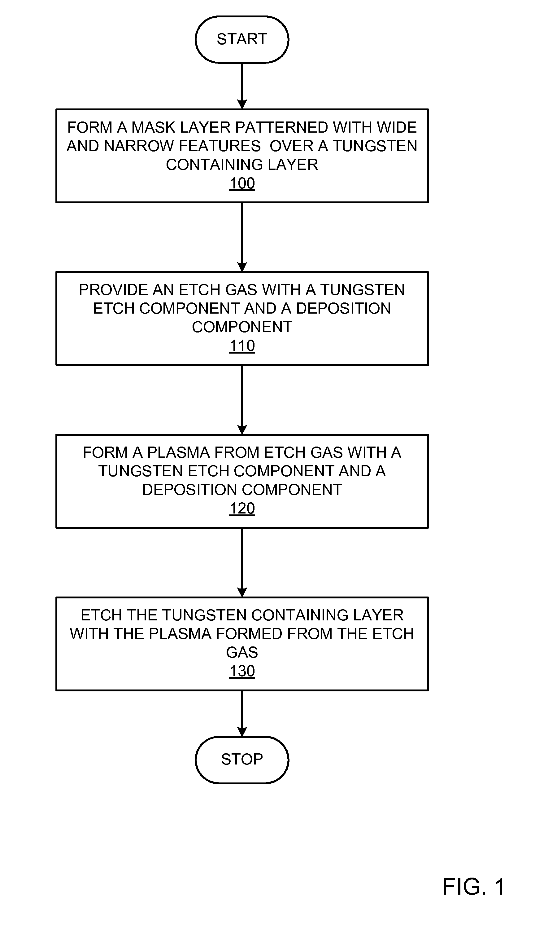
Method used
Image

Examples
Embodiment Construction
[0013]The present invention will now be described in detail with reference to a few preferred embodiments thereof as illustrated in the accompanying drawings. In the following description, numerous specific details are set forth in order to provide a thorough understanding of the present invention. It will be apparent, however, to one skilled in the art, that the present invention may be practiced without some or all of these specific details. In other instances, well known process steps and / or structures have not been described in detail in order to not unnecessarily obscure the present invention.
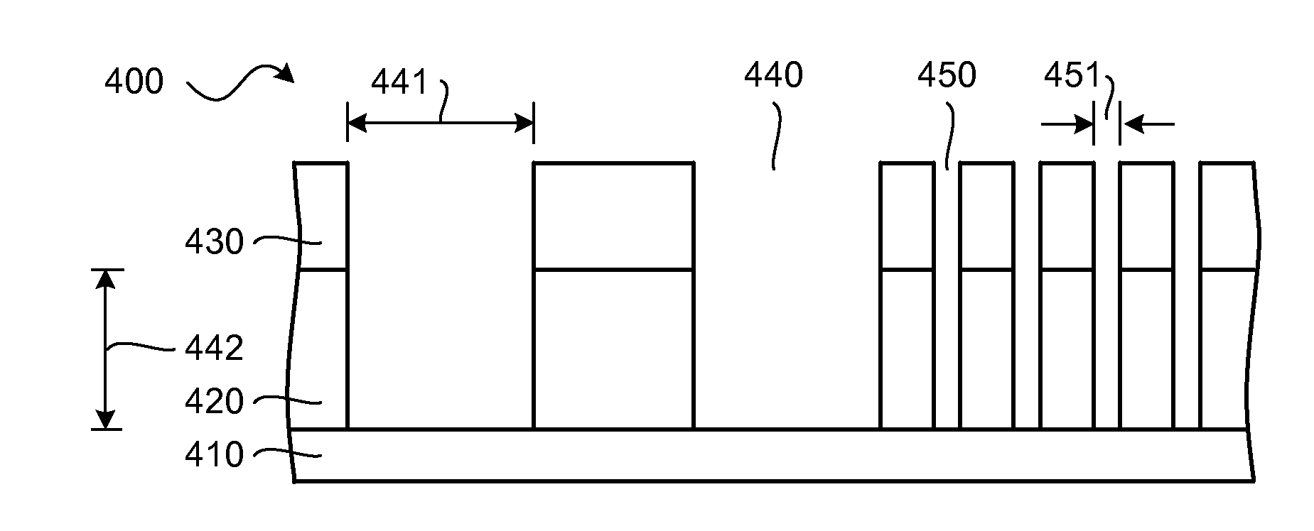
[0014]During the etching of semiconductor devices having features of different widths or different aspect ratios, and especially when the aspect ratios of the features are high, etch rate microloading is becoming a common problem. Due to diffusion limitations, the etching chemicals are able to go into the wider open features faster than into the narrower dense features. Similarly, the bypr...
PUM
| Property | Measurement | Unit |
|---|---|---|
| Plasma power | aaaaa | aaaaa |
| Etch rate | aaaaa | aaaaa |
| Aspect ratio | aaaaa | aaaaa |
Abstract
Description
Claims
Application Information