Thin film transistor array substrate, liquid crystal display device including the same and fabricating methods thereof

a technology of thin film transistors and array substrates, which is applied in the direction of semiconductor devices, instruments, electrical apparatus, etc., can solve the problems of reducing the width of the electrodes, and it is difficult to improve the aperture ratio of the pixel region, so as to improve the aperture ratio and facilitate the process of repairing the dark spot

Active Publication Date: 2011-06-30
LG DISPLAY CO LTD
View PDF4 Cites 62 Cited by
  • Summary
  • Abstract
  • Description
  • Claims
  • Application Information

AI Technical Summary

Benefits of technology

[0015]An object of the present invention is to provide a thin film transistor substrate, an LCD device including the same, and fabricating methods thereof that are adapted to improve the aperture ratio by forming a common electrode which overlaps a data line on a substrate.
[0018]Further still another object of the present invention is to provide an LCD device and a fabricating method thereof that are adapted to improve the aperture ratio by removing a black matrix opposite to a data line from a color filter substrate.
[0019]Furthermore, still another object of the present invention is to provide a thin film transistor substrate, an LCD device including the same, and fabricating methods thereof that are adapted to easily perform a process of repairing a dark spot without removing an organic insulation film.

Problems solved by technology

In addition, since the pixel electrodes and the common electrodes arranged in the pixel region are formed in a single metal layer, it is difficult to improve the aperture ratio of the pixel region by reducing the width of the electrodes.

Method used


Image

  • Thin film transistor array substrate, liquid crystal display device including the same and fabricating methods thereof
  • Thin film transistor array substrate, liquid crystal display device including the same and fabricating methods thereof
  • Thin film transistor array substrate, liquid crystal display device including the same and fabricating methods thereof

Examples


second exemplary embodiment

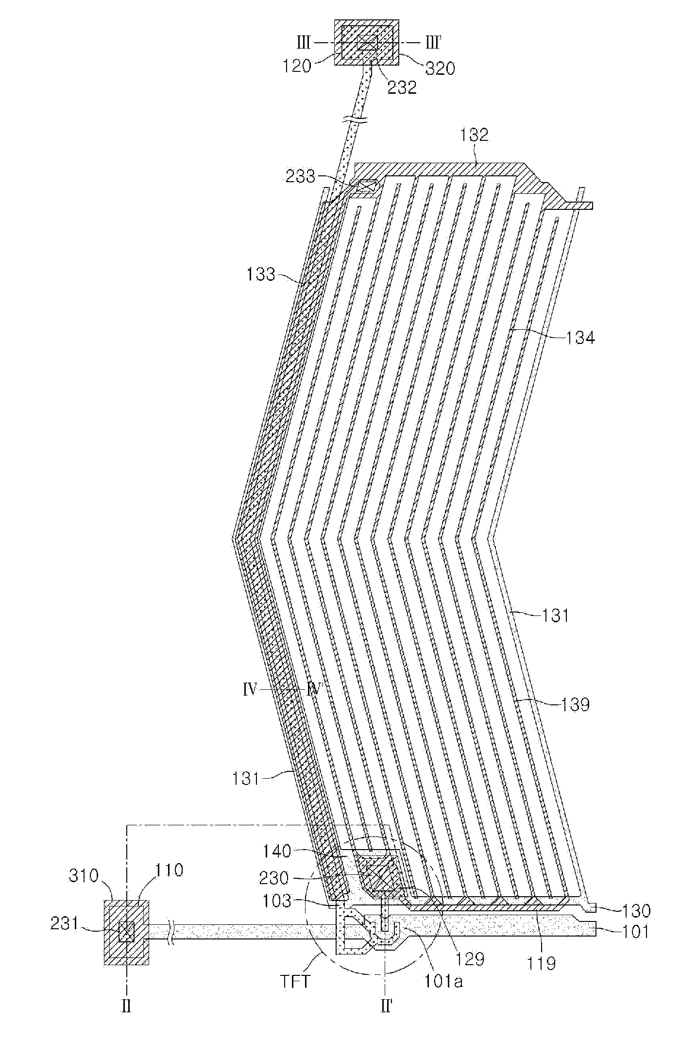
[0092]FIG. 9A is a view schematically illustrating a pixel region in an LCD device according to the present invention. FIG. 9B is an enlarged view schematically illustrating a thin film transistor in FIG. 9A. The LCD device of the second exemplary embodiment shown in FIGS. 9A and 9B may be configured in the same manner as that of the first exemplary embodiment. Therefore, the same elements in the LCD device of the second exemplary embodiment as those of the first exemplary embodiment in FIGS. 3A and 3B will be indicated by using the same reference numbers. Also, parts of the second exemplary embodiment distinguished from the first exemplary embodiment will be mainly described.

[0093]Referring to FIGS. 9A and 9B, the LCD device according to the second exemplary embodiment of the present invention forces a drain electrode 117b of a thin film transistor TFT and a first common line 430 not to cross each other. Therefore, a pixel repairing process can be easily performed for the LCD devic...

fifth exemplary embodiment

[0125]the present invention is applied to an LCD device of the FFS (Fringe Field Switching) mode. The FFS mode LCD device of the fifth exemplary embodiment may be configured in a similar manner to that of the second exemplary embodiment shown in FIGS. 9A and 9B, but differs from that of the second exemplary embodiment in a structure of the pixel electrode in the pixel region. Therefore, the same elements in the fifth exemplary embodiment as those of the second exemplary embodiment will be indicated by using the same reference numbers. Also, parts of the fifth exemplary embodiment distinguished from the second exemplary embodiment will be mainly described.

[0126]Referring to FIGS. 17A and 17B, the LCD device according to the fifth exemplary embodiment includes a pixel region defined by crossing a gate line 101 and a data line 103. A thin film transistor TFT is formed at an intersection of the gate line 101 and the data line 103. Also, a first common line 430 is formed to include a ben...


PUM


Abstract

A thin film transistor array substrate includes a substrate, a gate line and a data line arranged to cross each other and to define a pixel region on the substrate, a first common line disposed to be parallel to the gate line and to cross the data line, a switch element disposed at an intersection of the gate line and data line, a first pixel electrode formed to overlap the first common line, and a second pixel electrode branched from the first pixel electrode in a plurality of strips, a second common line opposite to the first common line in the center of the pixel region, a second common electrode branched from the second common line toward the pixel region into a plurality of strips, and a third common electrode branched to overlap the data line from the second common line, and a first storage electrode branched from the first common line into the pixel region, and a second storage electrode extended to overlap the first storage electrode from the first pixel electrode.

Description

[0001]This application claims the benefit of the Korean Patent Application No. 10-2009-0135681, filed on Dec. 31, 2009, and Korean Patent Application No. 10-2010-0045359, filed on May 14, 2010, which are hereby incorporated by reference in their entirety.BACKGROUND OF THE INVENTION[0002]1. Field of the Invention[0003]The present invention relates generally to a thin film transistor array substrate, a liquid crystal display (LCD) device having the substrate and fabricating methods thereof, and more particularly to a thin film transistor array substrate, a liquid crystal display (LCD) device having the substrate and fabricating methods thereof, which are capable of improving an aperture ratio of a pixel region.[0004]2. Background of the Related Art[0005]In general, an LCD device controls light transmittance of a liquid crystal with a dielectric anisotropy using an electric field, thereby displaying an image. The LCD device is usually fabricated such that a color filter array substrate...

Claims


Application Information

Patent Timeline
Patent Type & Authority Applications(United States)
IPC IPC(8): G09G3/36H01L33/08H01L21/336
CPCG02F1/134363G02F1/136213H01L27/1214G02F2201/40H01L27/12G02F1/136227H01L27/1288
Inventor CHOI, JUN HOCHO, HEUNG LYUL
Owner LG DISPLAY CO LTD
Why Eureka
Try Eureka