
Semiconductor memory device and method of operating the same

Active Publication Date: 2011-06-30
SK HYNIX INC
View PDF2 Cites 3 Cited by
  • Summary
  • Abstract
  • Description
  • Claims
  • Application Information

AI Technical Summary

Benefits of technology

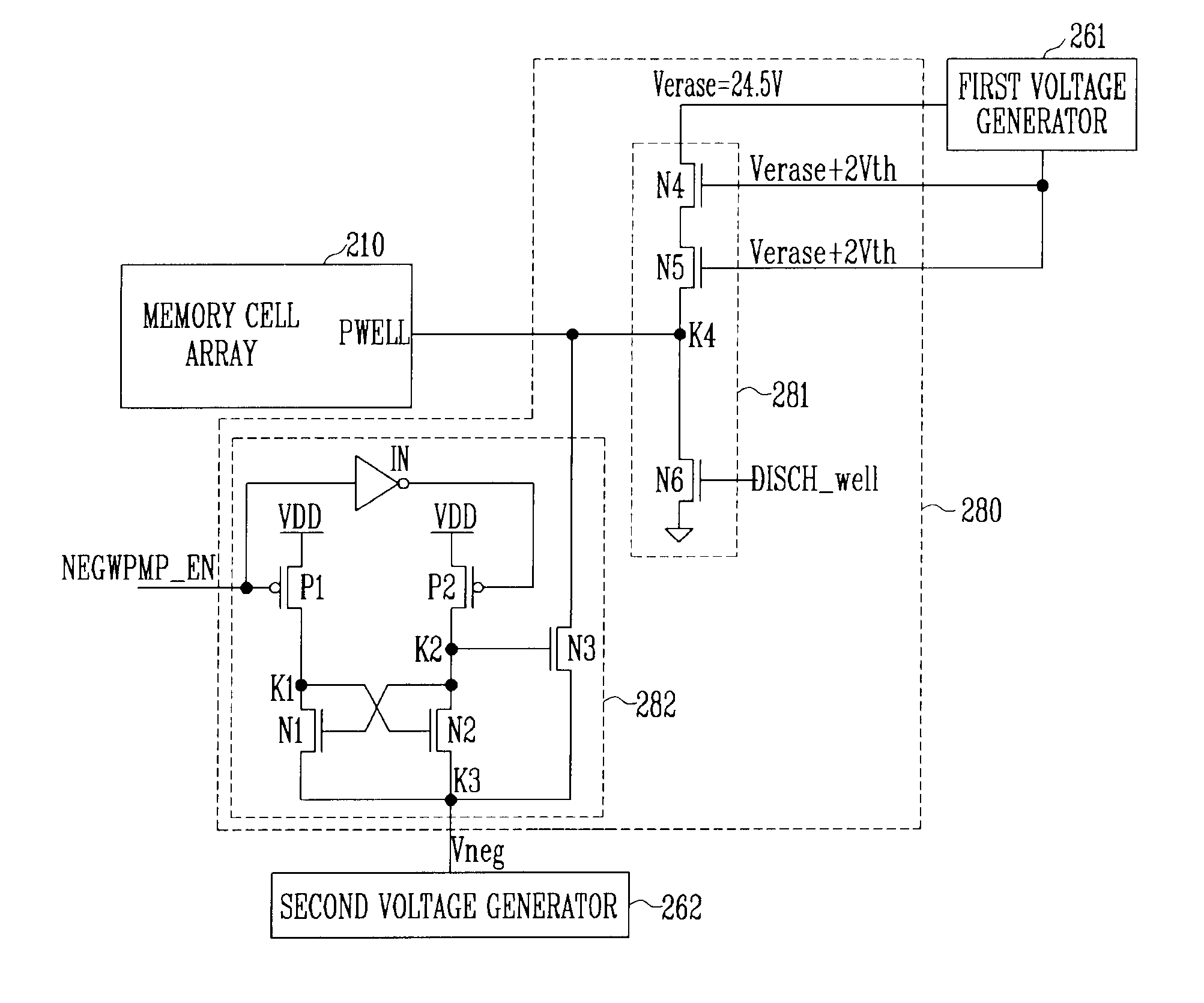
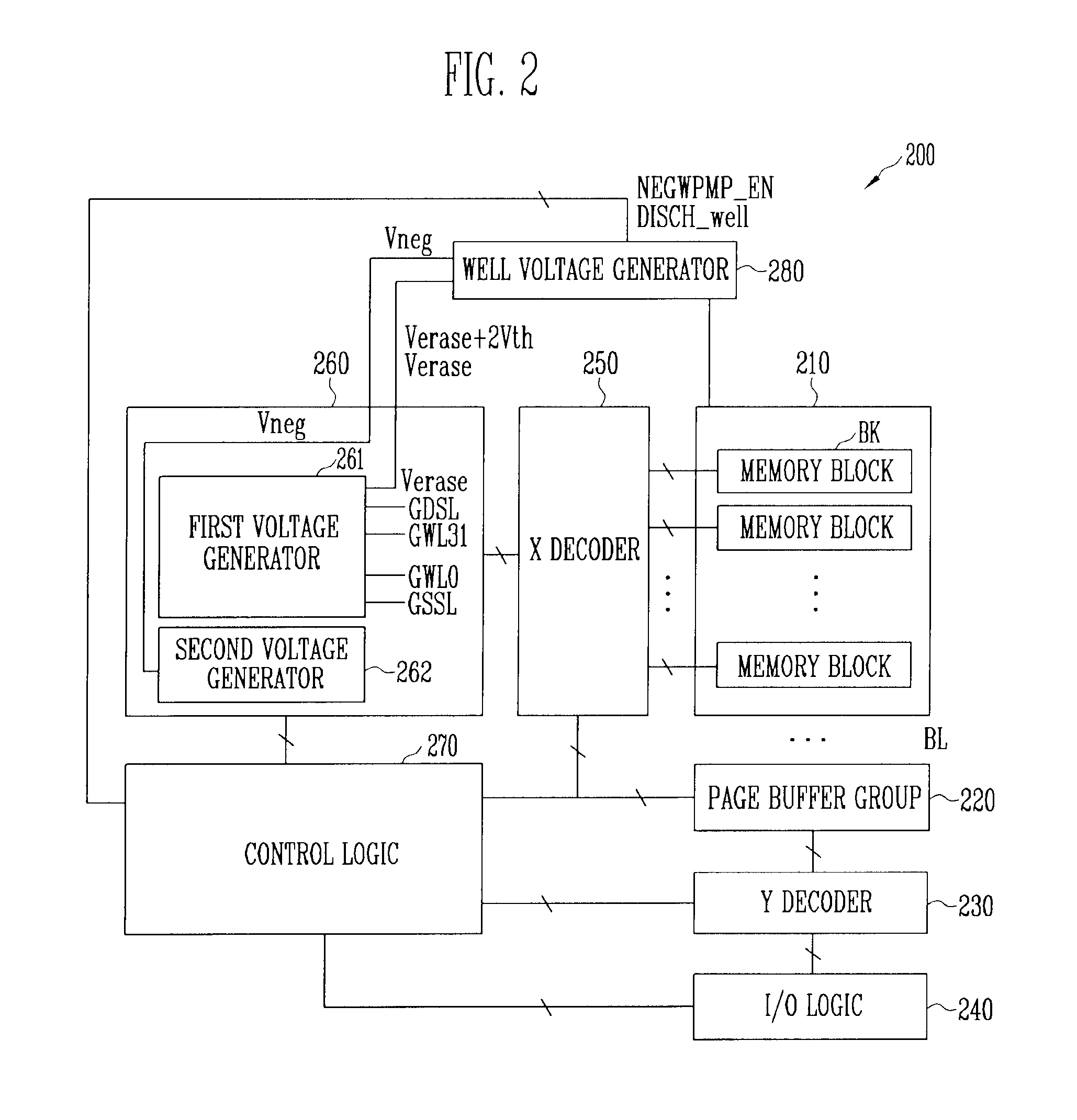
[0018]The second voltage generator includes a voltage level decoder for generating voltage level codes on the basis of negative voltage level information received from the control logic, a regulator for comparing the negative voltage and a target voltage determined by the voltage level codes and outputting a sense signal according to a result of the comparison, an oscillator for outputting first and second clocks in response to the sense signal, and a negative voltage pump for generating the negative voltage using the first and second clocks.
[0019]A semiconductor memory device according to another aspect of the presen

Problems solved by technology

Data stored in RAM is lost when power is not supplied.
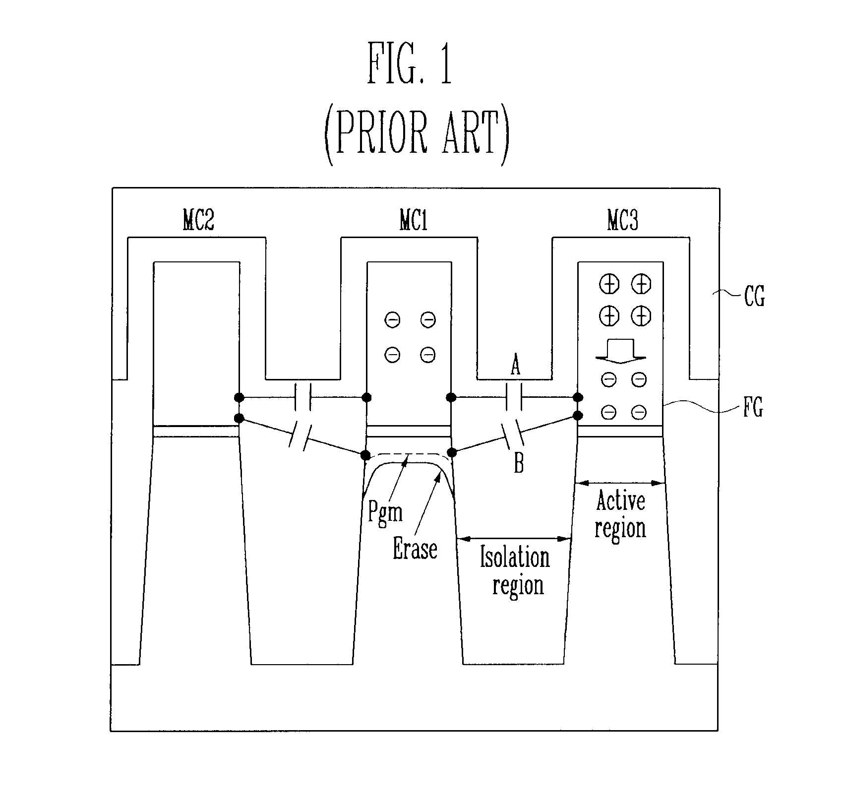
If the depletion region is reduced, current Ioff through a memory cell is increased even though it is turned off, and interference resulting from a bit line can become worse.

Method used


Image

  • Semiconductor memory device and method of operating the same
  • Semiconductor memory device and method of operating the same
  • Semiconductor memory device and method of operating the same

Examples


first embodiment

[0095]FIG. 5 is a timing diagram illustrating a program operation according to this disclosure.

[0096]Referring to FIG. 5, a program operation according to the exemplary embodiment of this disclosure is similar to a known program operation except that the negative voltage is inputted to the P well during a program operation.

[0097]More particularly, when the program operation is performed, the control logic 270 outputs the control signal to the first voltage generator 261 such that the first voltage generator 261 generates a program voltage Vpgm, verification voltages PV1 and PV2, and a pass voltage Vpass.

[0098]The control logic 270 outputs the reset signal NEGW_LOGRST, the data latch enable signal NEGW_DLE, the negative voltage information CTLBUS, the negative voltage pump enable signal NEGWPMP_EN, and the sense enable signal NEGWPMP_DET_EN to the second voltage generator 262.

[0099]The second voltage generator 262 starts generating the negative voltage Vneg as described above with re...

second embodiment

[0103]FIG. 6 is a timing diagram illustrating a program operation according to this disclosure.

[0104]Referring to FIG. 6, the negative voltage Vneg is not supplied to the P well during the time for which the program voltage Vpgm is supplied to the selected word line SEL WL as compared with FIG. 5. However, the second voltage generator 262 is already generating the negative voltage Vneg raised up to the target voltage level.

[0105]After the program operation voltage Vpgm is supplied and then discharged, the negative voltage Vneg is supplied to the P well. The verification voltages PV1 and PV2 are inputted to the selected word line SEL WL.

[0106]During the time for which the verification voltages PV1 and PV2 are supplied, the negative voltage Vneg continues to be supplied to the P well.

[0107]Assuming that the program operation according to the first embodiment of FIG. 5 is referred to as a first mode model and the program operation according to the second embodiment of FIG. 6 is referre...


PUM


Abstract

A semiconductor memory device includes memory blocks each comprising a plurality of memory cells formed over a semiconductor substrate having a P well, a first voltage generator supplying operating voltages to an selected block of the memory blocks, and a second voltage generator generating a negative voltage to the P well during a program operation.

Description

CROSS-REFERENCE TO RELATED APPLICATION[0001]Priority is claimed to Korean patent application number 10-2009-0135641 filed on Dec. 31, 2009, the entire disclosure of which is incorporated by reference herein.BACKGROUND[0002]Exemplary embodiments relate to a semiconductor memory device and a method of operating the same.[0003]Semiconductor memory devices are storage devices in which data can be stored and from which the stored data can be read as needed. The semiconductor memory devices are chiefly divided into random access memory (RAM) and read only memory (ROM). Data stored in RAM is lost when power is not supplied. This type of memory is called volatile memory. Meanwhile, data stored in ROM is not lost even when power is not supplied. This type of memory is called nonvolatile memory.[0004]The functions of semiconductor memory devices are gradually improved through the high degree of integration and an increase in the capacity and the chip size.[0005]Recently, in order to further i...

Claims


Application Information

Patent Timeline
IPC IPC(8): G11C16/04G11C11/34
CPCG11C5/147G11C16/3454G11C16/10G11C16/34G11C16/30G11C16/12G11C16/14
Inventor CHU, GYO SOO
Owner SK HYNIX INC
Features
  • Generate Ideas
  • Intellectual Property
  • Life Sciences
  • Materials
  • Tech Scout
  • Unparalleled Data Quality
  • Higher Quality Content
  • 60% Fewer Hallucinations
Learn More