Semiconductor device and method for manufacturing the same

Inactive Publication Date: 2011-07-07
SK HYNIX INC
View PDF4 Cites 7 Cited by
  • Summary
  • Abstract
  • Description
  • Claims
  • Application Information

AI Technical Summary

Benefits of technology

[0006]Various embodiments of the invention are directed to depositing an absorption barrier layer of a dielectric film on a semiconductor substrate including a bottom electrode contac

Problems solved by technology

The method of growing the HSG may have disadvantages when a critical dimension (CD) between the bottom electrodes is secured with a given standard.
Moreover, the HSG may peel of

Method used


Image

  • Semiconductor device and method for manufacturing the same
  • Semiconductor device and method for manufacturing the same
  • Semiconductor device and method for manufacturing the same

Examples


Embodiment Construction

[0036]The present invention will be described in detail with reference to the attached drawings.

[0037]FIGS. 1a to 1f are cross-sectional diagrams illustrating a semiconductor device and a method for manufacturing the same according to an embodiment of the present invention.

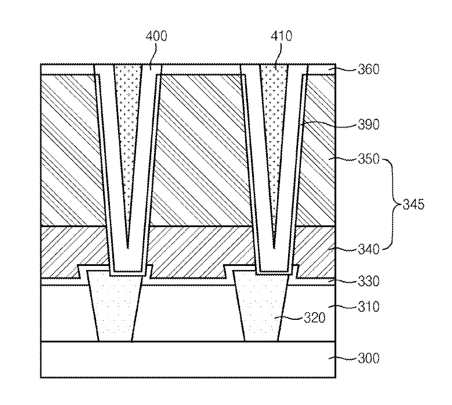
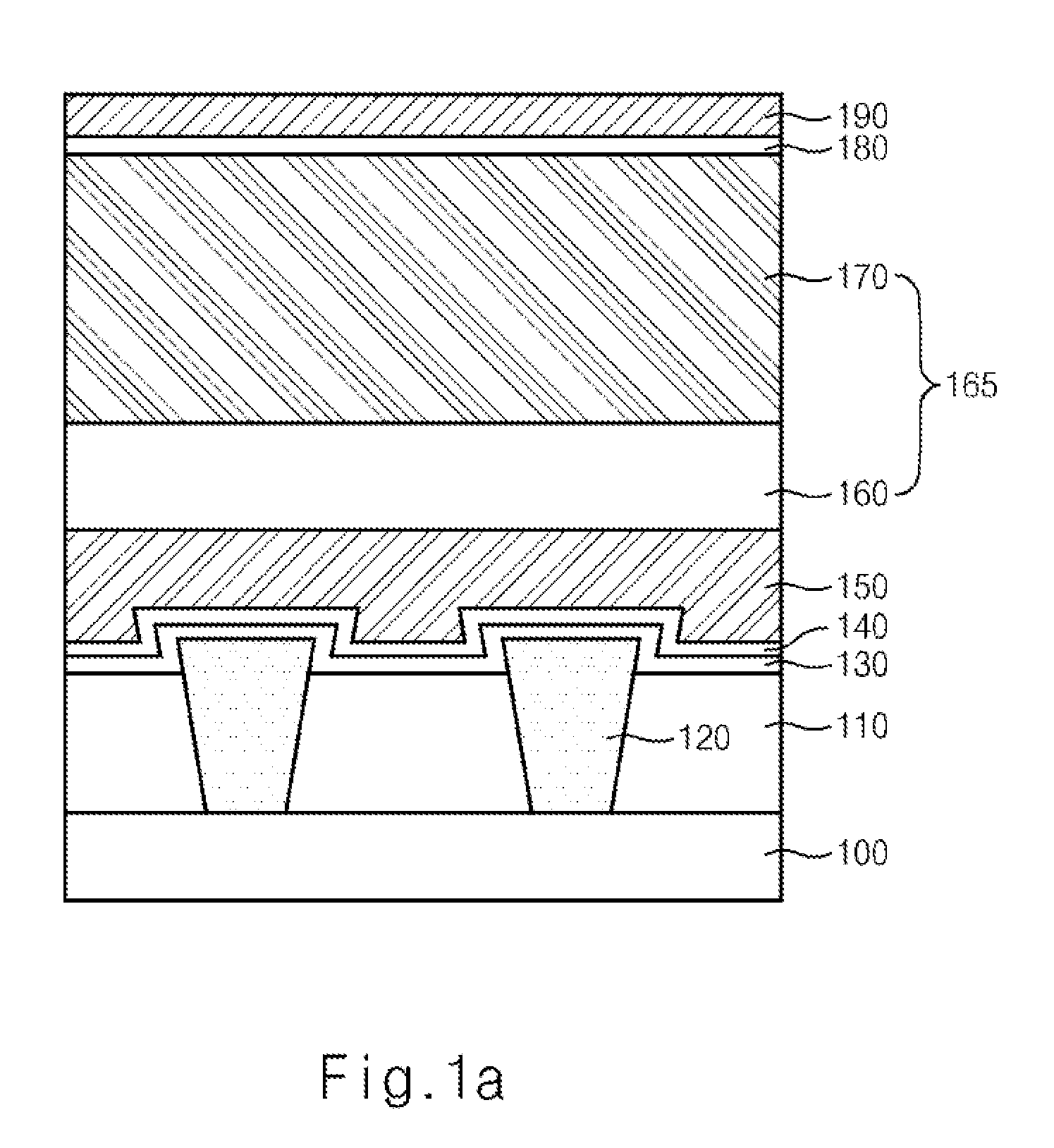
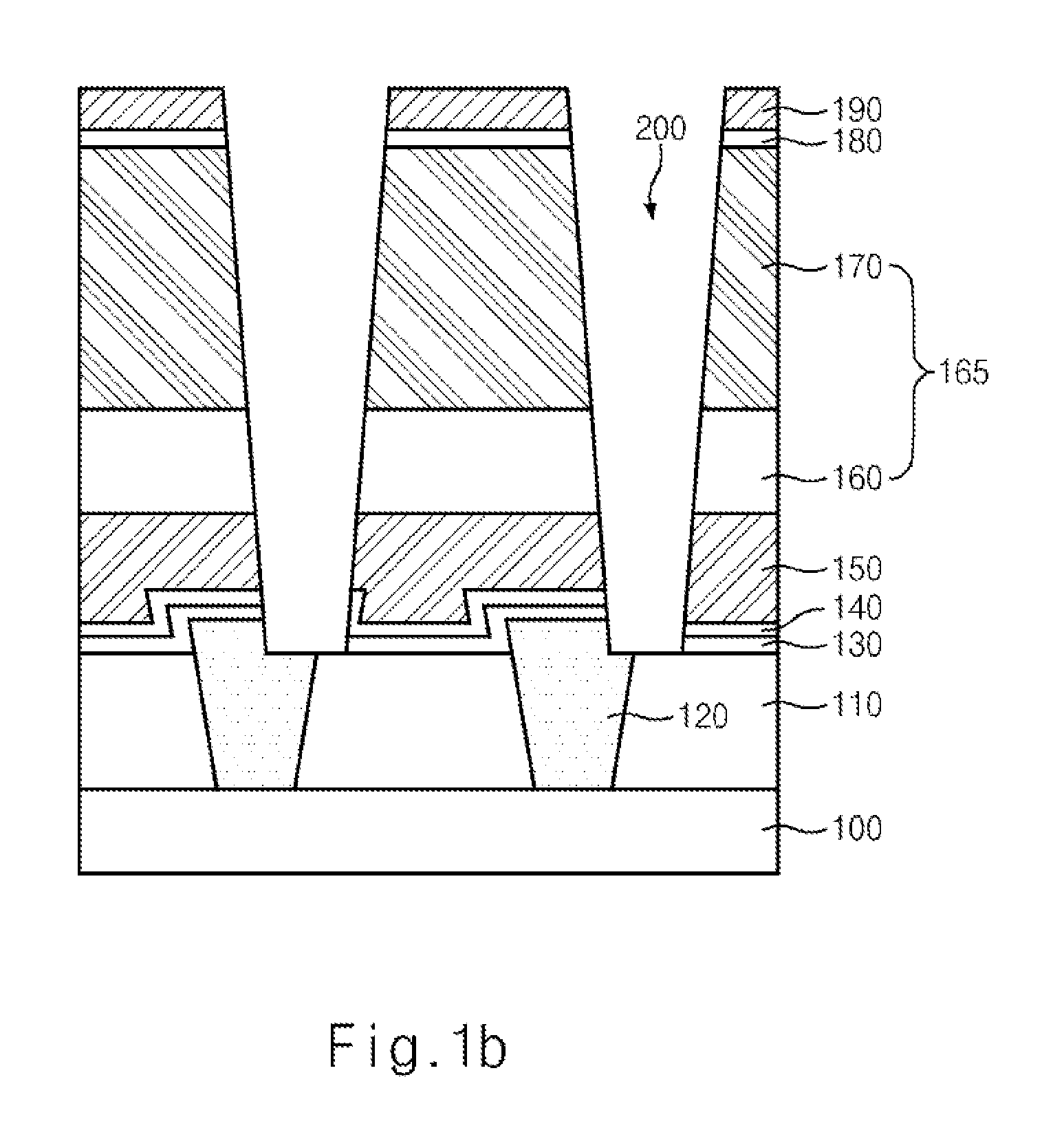
[0038]Referring to FIG. 1a, an interlayer insulating film 110 is formed on a semiconductor substrate 100. The interlayer insulating film 110 is etched using a bottom electrode contact mask to form a bottom electrode contact region (not shown). A conductive material is buried in the bottom electrode contact region to form a bottom electrode contact 120.

[0039]An etch stopper layer 130 is deposited on the interlayer insulating film 110 and the bottom electrode contact 120. The etch stopper layer 130 includes a nitride film.

[0040]An absorption barrier layer (or absorption prevention layer) 140 is deposited on the etch stopper layer 130. The absorption barrier layer 140 includes a Tetra-Ethyl-Methyl Amino (TEMA) materi...


PUM


Abstract

A method for manufacturing a semiconductor device comprises depositing an absorption barrier layer of a dielectric film on a semiconductor substrate including a bottom electrode contact plug so as to separate the dielectric films between capacitors without having any influence of a bias of the adjacent capacitor, thereby improving a refresh characteristic of cells.

Description

CROSS-REFERENCE TO RELATED APPLICATION[0001]The priority of Korean patent application No. 10-2010-0000771 filed on Jan. 6, 2010, the disclosure of which is hereby incorporated in its entirety by reference, is claimed.BACKGROUND OF THE INVENTION[0002]The present invention relates to a semiconductor device and a method for manufacturing the same.[0003]In the case of semiconductor devices like a DRAM, as the degree of integration increases, the area occupied by the device continues to decrease while a necessary capacitance is required to be maintained or increased. Generally, there are several methods to secure a sufficient cell capacitance in a limited area, these methods include using a high dielectric material as a dielectric film, reducing the thickness of the dielectric film or increasing the effective area of a bottom electrode. The method of using a high dielectric material requires physical and temporal investment like the introduction of new equipment, reliability of the diele...

Claims


Application Information

Patent Timeline
IPC IPC(8): H01L29/92H01L21/02
CPCH01L28/91H01L27/10852H10B12/033
Inventor PARK, HYUNG JIN
Owner SK HYNIX INC
Why Eureka
Try Eureka